If you’re like me and you’ve decided to take the plunge to learn KiCad – electronic design it can be real challenge. So when you want to start with KiCad remember everybody has to learn by taking steps before we can run.

KiCAD
KiCad is a tool that makes it possible to design high-quality printed circuit boards. It is not the only one, in fact there are many many other tools out there. Some are free, some are very expensive, and each tool has its advantages over others. Software tools that help people make printed circuit boards are often referred to as “Electronic Automation Design” tools, or “EDA” for short.
INSTALLATION
There is KiCad support for many other operating systems as well, including downloading the source code and compiling from the source code if you know how to do that. Here, we’ll keep it simple and install the already compiled version. Let’s go into the Mac OS X branch, and there are two types of downloads that you can do; the recent builds and you can build from source.
Download the Kicad installation files for Mac OS X from http://kicad-pcb.org/download/osx
As far as the recent build is concerned, there’s a slight difference to how this works for Windows. There are two big files you can download. The first one is KiCad.dmg and the second one is KiCad-extras.dmg. The first file contains KiCad itself, documentation, the schematic symbols, and some templates, but it doesn’t contain any footprints. So you’ll be getting the footprints from the Kicad GitHub repository. To do that, you obviously need a live Internet connection. If you find yourself working offline, like traveling on a train or a bus, like I find myself sometimes doing, then you will also need to download KiCad-extras.dmg and this contains the footprints that you can use offline.
For more information about installing KiCAD go here.
SCHEME
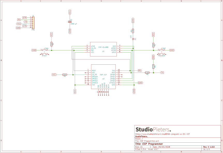
The process begins with Eescema. In Eeschema we create the electrical schematic that describes the circuit that eventually will be printed onto the PCB board. We draw the schematic by picking components from the library and if a component that we need doesn’t exist in the library, we can create it using the schematic library editor. I took my previous project ESP8266 – PROGRAM A 01 & 12F to make a pcb for easy programming my ESP modules. As you can see I made the scheme according my breadboard setup.
PCB
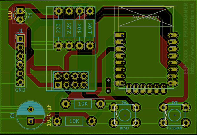
We use Pcbnew to place the footprints on the blank canvas, and then do the wiring. We can move the components around so that they are nice and tidy and we’ll start doing all the connections between the various pins using. This process is very time consuming, especially for large projects. The placing and routing is mostly a manual process. Although Kicad does have an auto router, most people prefer not to use it, in favour of the manual process which give the designer absolute control.

Once you have your PCB laid out and connection’s completed you can go ahead and do a design rules check that’s going to make sure that, for example, a track’s not too close to a pad and things like that. Look for any pads that are not connected and things of that sort. We can always fix footprints using the footprint editor.
GERBER FILES
Assuming that you are finished with the current iteration, you will want to have it fabricated. To do that you must export the PCB data as a collection of files, called “Gerber files”. I will describe Gerber files in more detail in the next chapter. Gerber files contain several related files, with one Gerber file per layer on your PCB and contains instructions that the fabrication house will need in order to make your PCB.
One thing to notice about the Kicad design process is that it has a lot of closed loops; there is a lot of iteration happening. As we’ll see in the first example project, It is often the case where you go into your PCB design and then you realize that there is a component you should have included in your schematic design in Eeschema but then you forgot about it or you just didn’t think it would be necessary until later in the process. In this case you can go back to Eeschema, adjust the schematic with whatever was missing or make your additions or changes and then go and create a netlist and go back to Pcbnew to continue your layout work there. There is a lot of iteration that is happening here. This is ok! It’s not that hard to be iterative in Kicad; the workflow allows you for that.
PRODUCTION
Now that I made the necessary files to really produce the PCB’s I need a manufacturer. I found one that makes 10 PCB’s for only USD$4.90 !
Seeed is a hardware innovation platform tailored for makers to help grow inspirations into differentiating products, by providing accessible technologies with quality and delivery guaranteed. Seeed Fusion Service offers one-stop prototyping services for PCB (Printed Circuit Board), PCBA (PCB Assembly) and other electronic and mechanical customized services such as CNC Milling, 3D Printing and PCB Layout services. Seeed Fusion promises mature PCB manufacturing and fabrication with affordable prices, competitive lead times and 100% quality guaranteed. If you are not satisfied with the final product or service received, we will be sure to do our best to make it right. You can count on us to cater to your specific PCB needs, from the simplest of boards to the most complex designs for small quantity and large scale production. We can handle laser drilled microvias, via-in-pads, heavy copper up to 20 oz, up to 40 layers, cavity boards, microwave and RF boards and more. Get high quality boards starting from just $4.90. You can find more information here.

If you also want to make your own PCB’s I would recommend to start here, this is a great step by step manual.
I can’t wait until I receive my PCB’s! I will post a picture when I receive them.
DO YOU HAVE ANY QUESTIONS? LEAVE A COMMENT DOWN HERE.
REFERENCE
Tech Explorations (Mar 16 2016), KiCAD LIKE A PRO, This course is designed to teach you how to use KiCad assuming no prior knowledge in PCB design. , http://kicad.txplore.com/index-p=185.html SEEED Studio (2008-2018), FUSION PCB MANUFACTURING, Fusion offers one stop prototyping services for PCB (Printed Circuit Board) , https://www.seeedstudio.io/fusion_pcb.html