For anyone out there who has ever struggled finding a part for KiCAD, there are some who would say you’re doing it wrong. You’re supposed to make your own parts if you can’t find them in the libraries you already have. This is really the only way; PCB design tools are tools, and so the story goes you’ll never be a master unless you can make your own parts. In my previous blogs here I showed you how to create a Symbol, now we going to make our footprint.

KiCAD PCB Footprint
A footprint or land pattern is the arrangement of pads (in surface-mount technology) or through-holes (in through-hole technology) used to physically attach and electrically connect a component to a printed circuit board. The land pattern on a circuit board matches the arrangement of leads on a component.
Component manufacturers often produce multiple pin-compatible product variants to allow systems integrator to change the exact component in use without changing the footprint on the circuit board. This can provide large cost savings for integrators, especially with dense BGA components where the footprint pads may be connected to multiple layers of the circuit board.
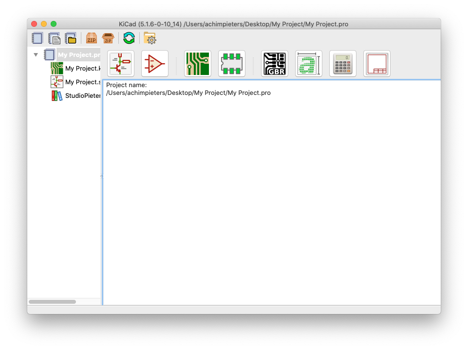
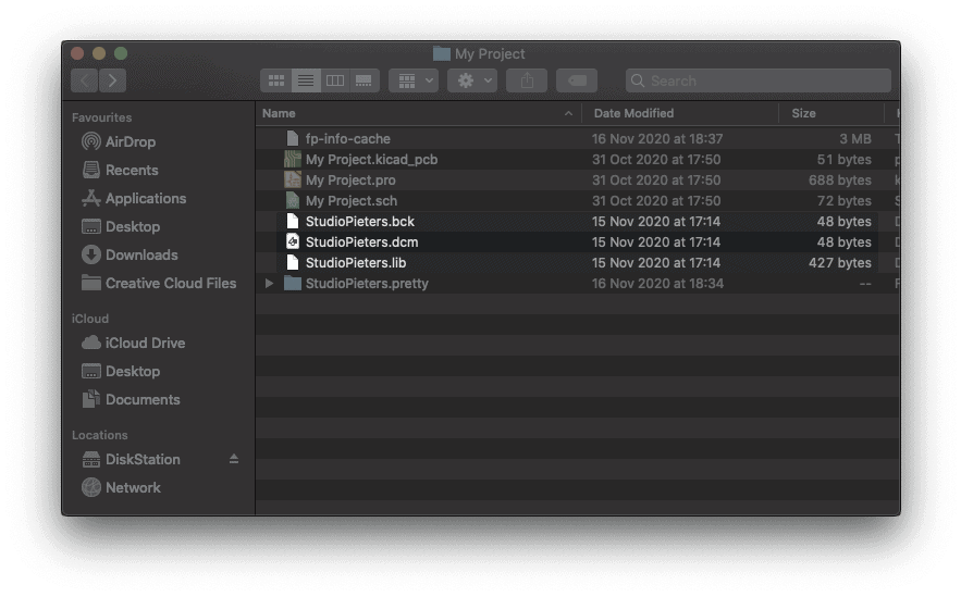
Open you saved project in KiCAD
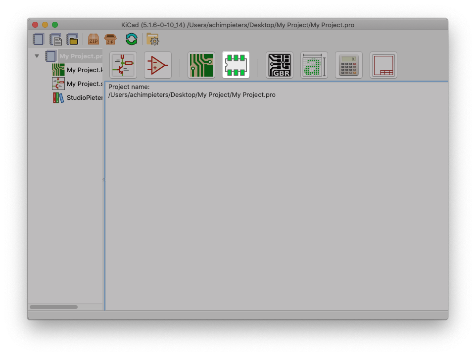
 Open the ‘Footprint Editor’ by clicking the IC component symbol.
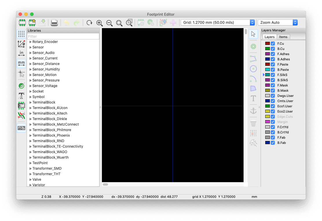
A new window will appear.
Note: In the previous blog Schematic Symbol, I didn’t load the default Symbols library at the installation, so the left pane was empty! Normally you will see here all available libraries as shown below.
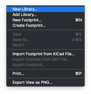
 Now click ‘File’ in the top menu bar and select ‘New Library’.
 Enter the name of your new library (eg StudioPieters).And select where you want to save it (eg My Project).
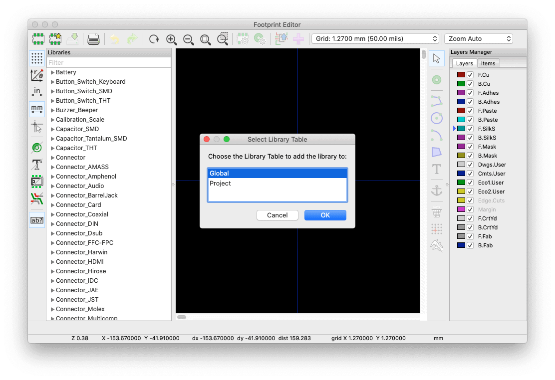
Now you have to options save it as a new symbol only for this project or global as it can be used in other projects. I chose Global.
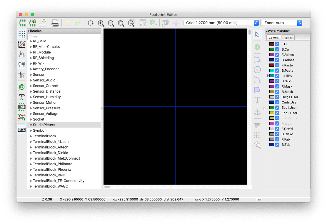
 Now you will return to your previous screen and as you can see in the left pane we have created a new library.
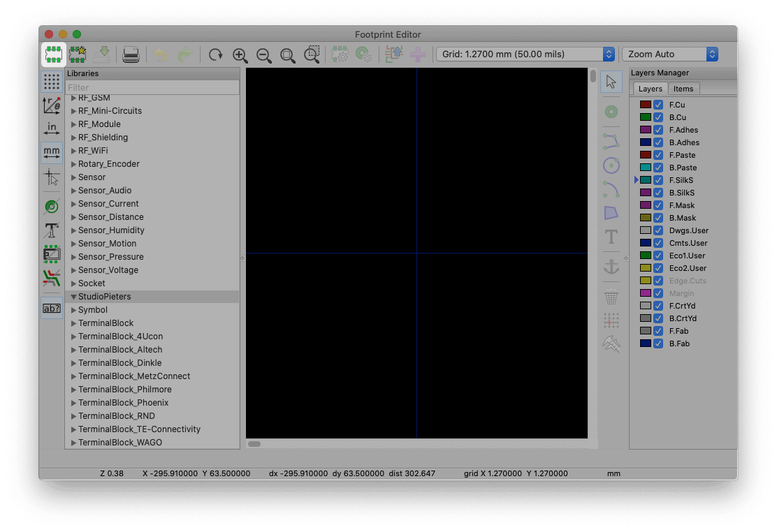
 Now we can add our new symbol to our newly created library by clicking the IC component symbol in the left upper corner.
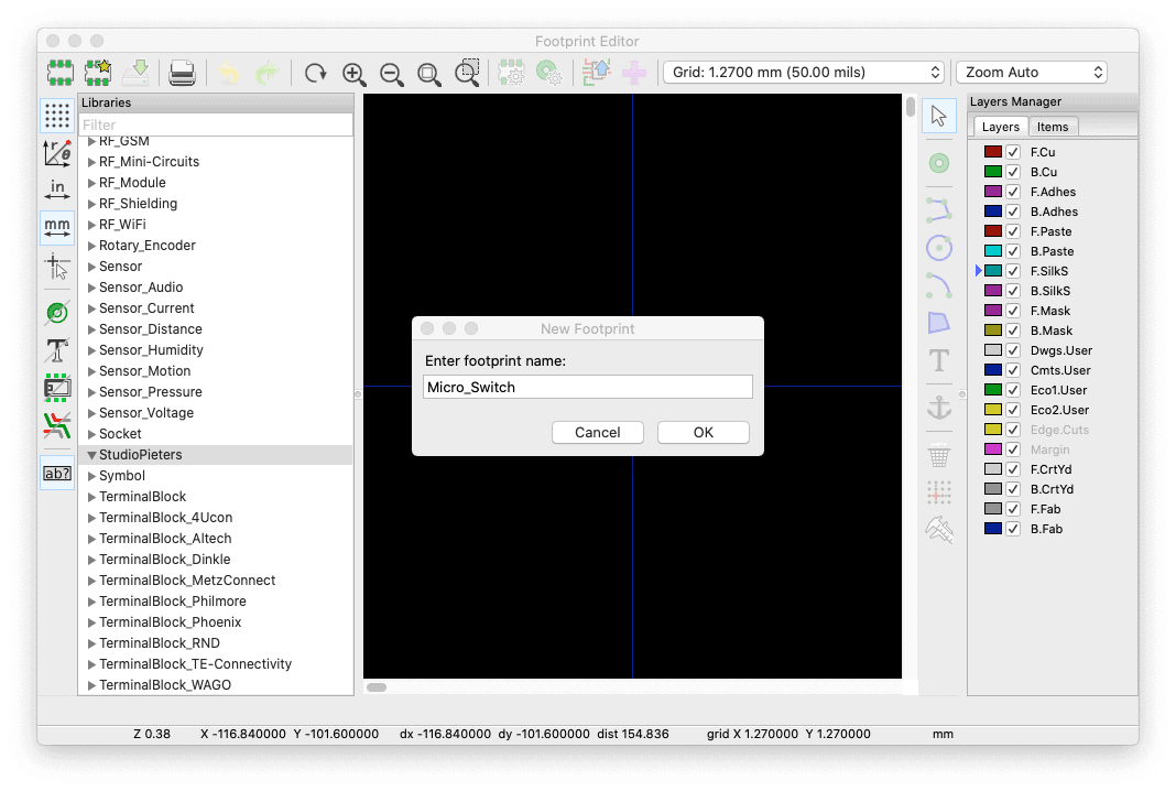
 Now you will be asked to enter to footprint name (eg Micro_switch).
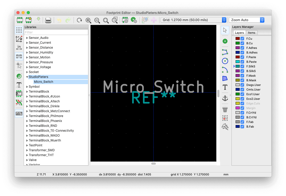
Now we have created our base file. As you can see in the left pane a new footprint has appeared ‘Micro_Switch‘. and in the right pane we see the text we just entered. In this pane we are going to draw our new footprint.
 To draw our footprint I use the data sheet land pattern as a guide.

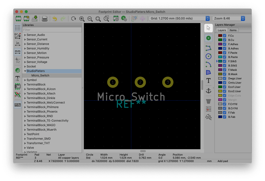
 Click on the ‘add pad‘ on the right side of the screen.
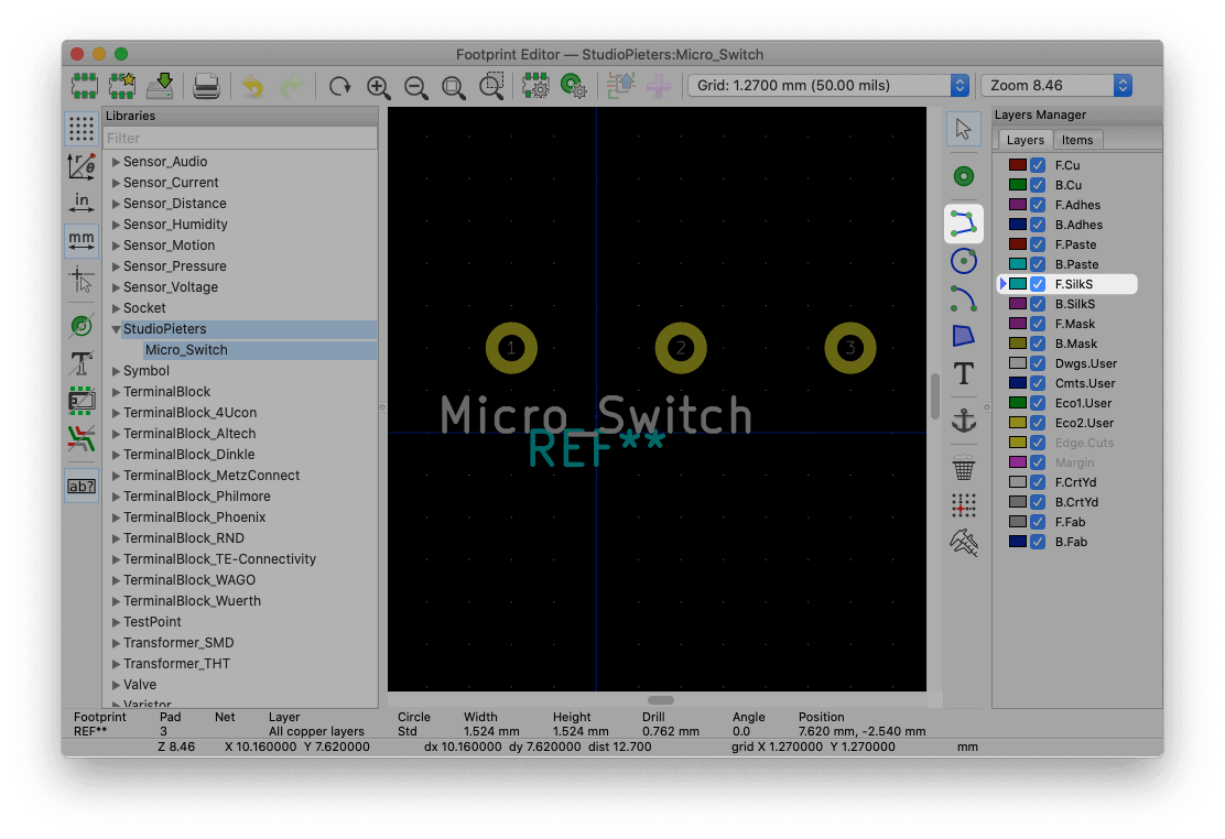
 Place three pads in the drawing.

 Click on the ‘Select item‘ on the right side of the screen.
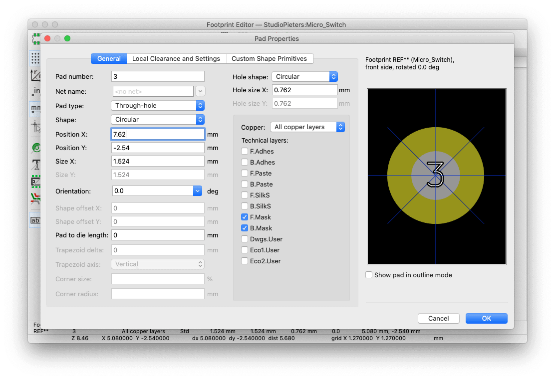
We start with the first pad called ‘1‘. Double Click on the image to see the settings you need to create the symbol. A new window will appear. In this window we can adjust the settings we need to adjust our footprint. See image for reference. We also do this for pad 2. See image for reference.
 And for Pad 3. See image for reference.
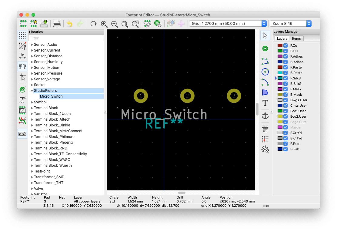
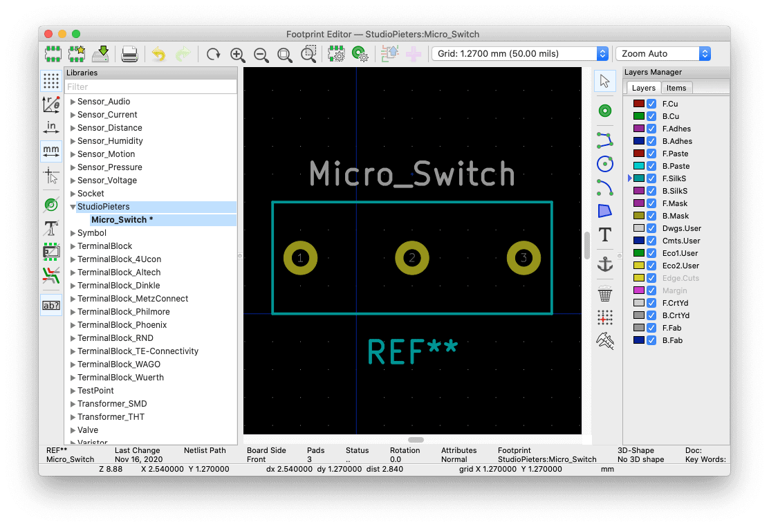
 Your Footprint should look like something like this.
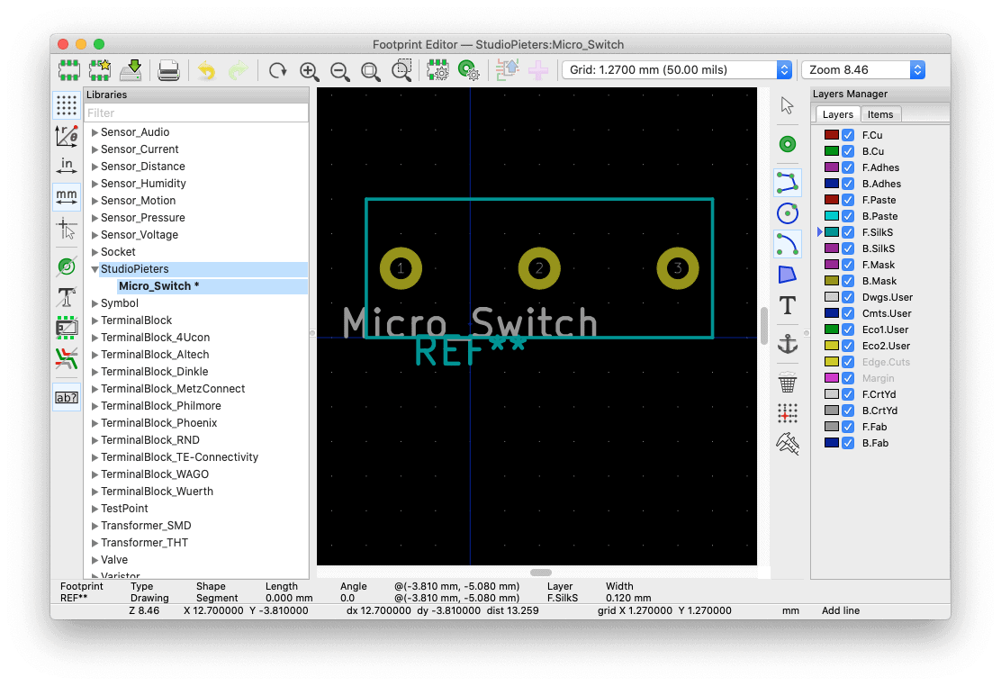
 Click on the ‘Add Graphics line‘ on the right side of the screen.
 Draw a rectangle around the placed pads.

 Click on the ‘Select item‘ on the right side of the screen.
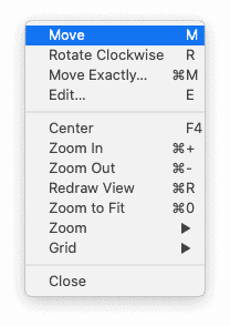
 Hold down the ‘CTRL‘ button and click on the text. A drop down menu appears and select ‘Move‘.
 Move your text to the wanted position.
 Now we have created our footprint, now we only need to save it by pressing the save button in the top menu.
 See you in the next blog where I will explain how to make the 3D Model.
 REFERENCE
KiCAD, KiCad EDA (2021),A Cross Platform and Open Source Electronics Design Automation Suite, https://kicad.org Autodesk Fusion 360, Download Fusion 360 for free (2020), Fusion 360 for free with a 30-day trial. Access all capabilities and features with integrated CAD, CAM, CAE, and PCB software.,https://www.autodesk.com/products/fusion-360/free-trial