In this blog, I will learn you how to Create a new symbol (or component as it is also known). You use symbols in schematic diagrams that you can create in Eeschema. Most likely, you want to create a custom schematic symbol because you have a physical component but can’t find an existing symbol to represent it. Perhaps you have searched through the symbols that come with Kicad, and Googled for suitable third-party symbols, but couldn’t find any.

It is also likely that you will want to associate your new symbol with a footprint. If your physical component has a standard package, like DIP, for example, then you will be able to associate an existing footprint with your custom symbol. If not, you will also need to create a custom footprint.
In this blog, you will learn how to create a custom symbol by creating a symbol for the 555 timer integrated circuit. There are plenty of libraries for Kicad that contain this symbol, but for the sake of learning, let’s pretend that we can’t find it. What we want to create is a symbol like the one in the Figure.

Our objective is to create a symbol that complies with convention. In regards to IC symbols:
- We arrange pins around a rectangle.
- We group pins according to function (like inputs, outputs, power etc.)
- We place the Vcc pin on the top of the rectangle.
- We place the GND pin on the bottom of the rectangle.
- We choose an appropriate name and designator for the symbol.
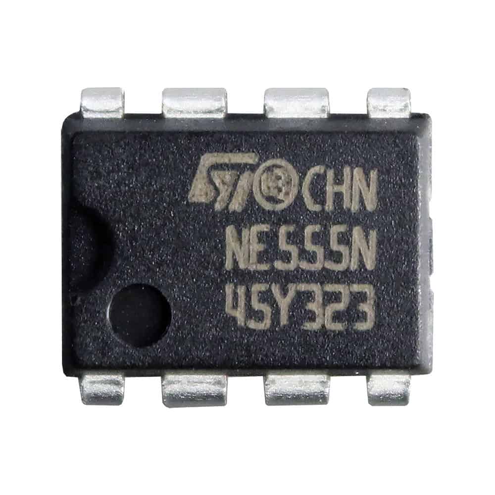
The physical component that we are working with is in this Figure . This component comes in a standard DIP package with 8 pins.
Because we are working to create a symbol, we don’t need to know anything about the physical characteristics of the physical component other than the total number of pins that its package contains. You need to know details about the physical characteristics are essential when you are working on the footprint of the component.
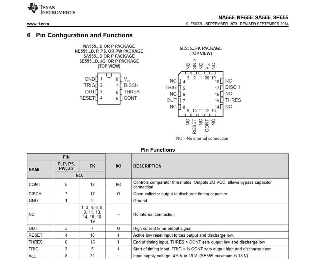
However, it is beneficial if you have access to the components data sheet. The data sheet contains information that you need: The names, numbers, and roles of each pin, whether they are input, output, bidirectional, power, signals, etc. All this is useful information, and the more you have on hand, the better.
The data sheet for the example component is available from its manufacturer. The information you need is on page 6.
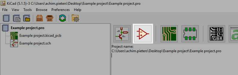
Let’s start the process of creating a new symbol. In the main KiCAD window, click on the Symbol Library Editor button. you can do this by selecting “Tools” in de menu bar and then select “Edit Schematic Symbols” or press the “Edit Schematic Symbols button” .
You must store each symbol inside a library file, so before you start creating the symbol create a new library. Create a new library by clicking on the “New library” button or through the “File” menu file “New library”
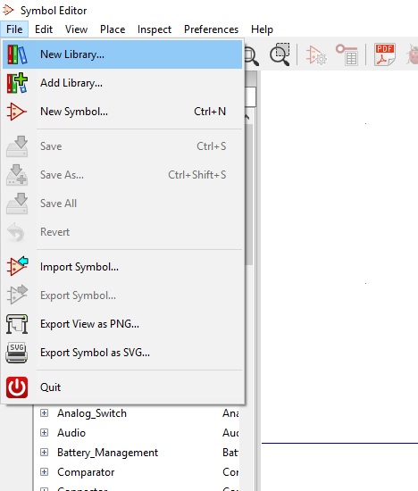
Create a new symbol library eg. “StudioPieters_library”.

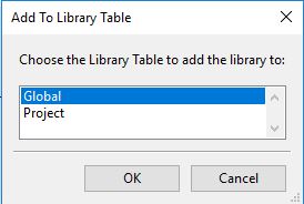
KiCAD will ask you if you would like this library to be available to all projects (“Global”) or only to the current project (“Project”). Choose the most appropriate one for your circumstances (I chose “Global”). You are now working in the new library, and you will store the new symbol in it.
You can confirm this by looking at the header of the Editor window. The path and name of the library you just created must be showing there. Next, click on the “Create new symbol” button in the top toolbar.
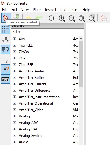
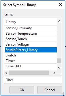
A prompt will ask you to select the library in which you will store the symbol. The library you just created should be listed. Click on it to select it and click “ok” to continue.
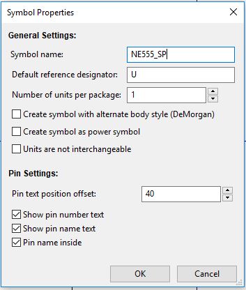
The Symbol Properties window will show up. The most important values that you need to complete are the symbol name and designator. The name typically consists of the physical component’s model name and any other information that helps to identify it. When you use it later, you have to search for it in the symbol library and having a good name will help you find it quickly. In my example, because I want to differentiate my 555 symbol to those that exist in other libraries, I add some extra text “_custom” at the end of the name.
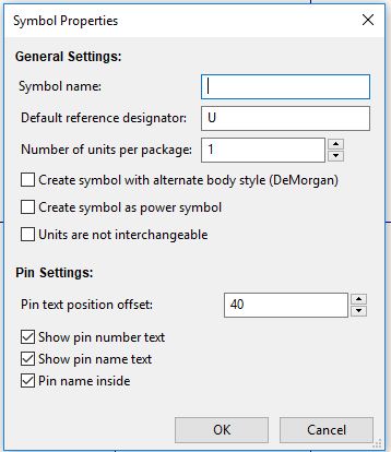
For the designator, you should not guess. Visit Wikipedia to see the Reference Designators table. The designator for integrated circuits is “U” so type this in the Default Reference Designator field. Below, shows the values I have entered in the Symbol Properties window. Other than the symbol name and the designator, everything else remains as per the default.
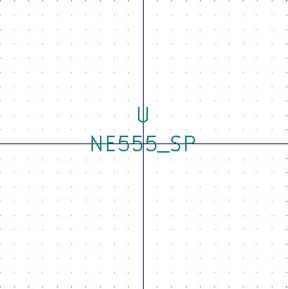
Click Ok to commit and continue. Kicad will place the designator and symbol name in the middle of the sheet, on top of the other. Use the “M” hotkey to relocate the two blocks of text. You should have something similar to the example in Figur.
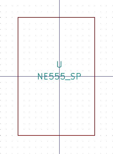
Continue by drawing the outline of the symbol. You can either use the polygon tool or the rectangle tool:
![]()
Your outline should be somthing like this.
Add the background color that is consistent with other IC symbols by opening the drawing properties window for the rectangle (place your mouse pointer on the rectangle line and type “E”).
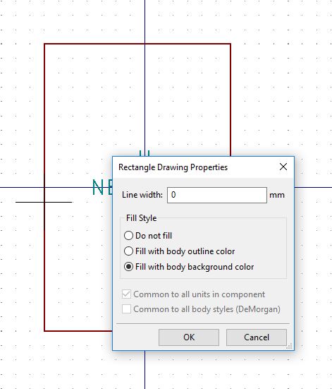
Under “Fill Style”, check the “Fill background” radio button.

Next, work on the pins. Keep the datasheet open because you need the information in it. For your convenience, refer to the excerpt . Click on the pin button in the right toolbar![]()
Place the 8 pins around the perimeter of the symbol outline, as in the example below. The thing to remember here is that the convention is to group similar pins together and place the two power pins to the top and bottom of the rectangle. Let’s start with the Vcc pin. According to the datasheet, the Vcc pin is number 8, and according to the convention, it should go to the top edge of the rectangle. Click on the pin tool, and then click in the middle of the top edge. The Pin Properties window will come up. Fill it as you can see in the example.
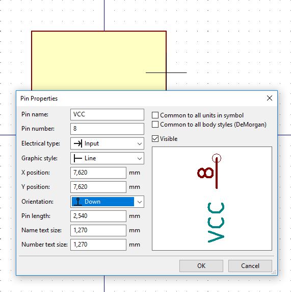
The fields inside the box are the ones that you need to focus on. The pin name is arbitrary, but of course, you should use a name that is appropriate. I usually use the same name that I see in the documentation for this pin. The Pin number, on the other hand, is very important. The Pin number is how schematic symbols and footprints can associate physical and symbolic pins.
In the orientation drop-down, select the option that matches the side of the rectangle where you are attaching the pin. The Vcc pin should go on the top of the rectangle and should have its circular connector pointing away from the rectangle. The horizontal line of the pin orientation icon represents the rectangle. If you wanted to place the pin on the left of the rectangle, you would choose the icon with the circular connector printing towards the left.
Finally, because the Vcc pin is a power pin, I have selected the “Power input” electrical type. You should choose the same type for the GND pin.
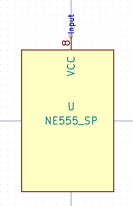
Click Ok to commit the changes. Please the pin in the middle of the top side of the rectangle, as you can see in Figure. I have moved the text block so that they don’t overlap with the pin.
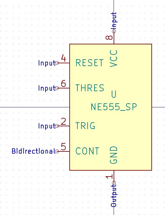
Follow the same process to add the GND pin (pin 1) in the bottom edge of the rectangle. Copy the pin name and number from the datasheet, and mark it also as a Power Input.
Continue with the left side of the rectangle where you should place the input pins. According to the datasheet, the input pins are RESET, THRES, TRIG. There is one bidirectional pin, “CONT,” which you can place either on the left or the right of the rectangle. I have placed it on the left.
The pin attributes for the input pins on the left of the symbol look like the example. Remember that pin 5 is bi-directional so its electrical type should be “bidirectional”.
Continue in the same way to create the last two pins. Those are output pins, as per the datasheet. When completed, you should have a symbol that looks like the example.
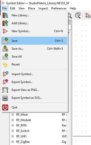
Your work is complete. Save the symbol to the selected library by clicking on the Save Current Symbol button:
Then, test that you can use it in Eeschema. Open Eeschema. Go into Symbol Libraries from the Preferences menu and add the new library. Place your cursor on the Sheet and type “A” to add a new symbol. Search for the name of your library by typing part of its name in the filter field. The library should appear. Double-click on the symbol to drop it on the sheet.
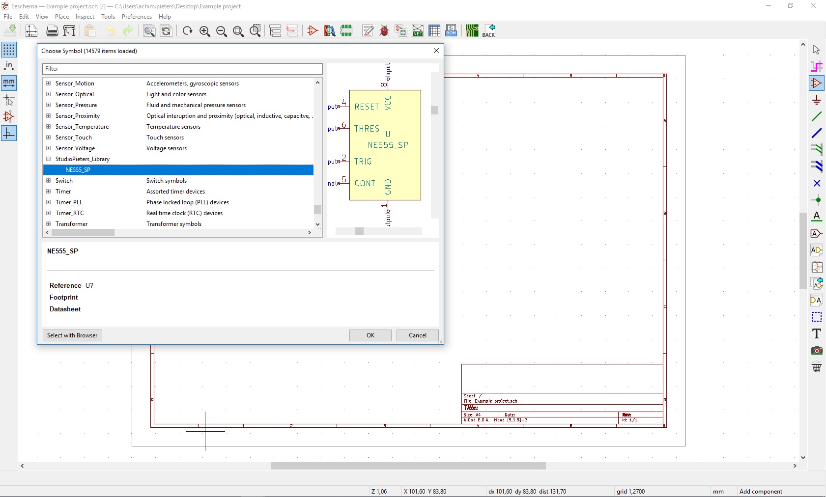
The custom 555 symbol should now be in place inside Eeschema, and you can go ahead to use it as you do with any other symbol. In this blog, I showed you how to create a brand-new symbol.

REFERENCE
KiCAD,A Cross Platform and Open Source Electronics Design Automation Suite, https://www.kicad-pcb.org Tech Explorations Inc., Kicad 5 recipe: How to create a new component (symbol),https://techexplorations.com/blog/kicad/blog-kicad-5-recipe-how-to-create-a-new-component-symbolg