Hand soldering Surface Mount Devices (SMD) scares a lot of Makers, but it is easier than what it looks like. Even sometimes, it’s easier than soldering Through Hole Components. Really! The Components are naturally held in place by their legs, while SMD are just sitting flat on the PCB, only waiting for the smallest PCB move, to fly away. And, as small and lightweight they are, they fly pretty well and pretty far away! My first tryouts were disastrous, usually ending by a poor resistor, fried on my iron tip…So, we need to keep the small component stuck in place, without the need of a third or fourth hand. Let jump in, but first some background information.

Surface Mounted Device
Surface Mounted Device (SMD) is a method for producing electronic circuits in which the components are mounted or placed directly onto the surface of printed circuit boards (PCB’s). An electronic device so made is called a Surface Mounted Device (SMD). In industry, it has largely replaced the through-hole technology construction method of fitting components with wire leads into holes in the circuit board. Both technologies can be used on the same board, with the through-hole technology used for components not suitable for surface mounting such as large transformers and heat sinked power semiconductors.
By employing SMD, the production process speeds up, but the risk of defects also increases due to component miniaturization and to the denser packing of boards. In those conditions, detection of failures has become critical for any SMD manufacturing process.
An SMD component is usually smaller than its through-hole counterpart because it has either smaller leads or no leads at all. It may have short pins or leads of various styles, flat contacts, a matrix of solder balls (BGA’s), or terminations on the body of the component.

Component Identification
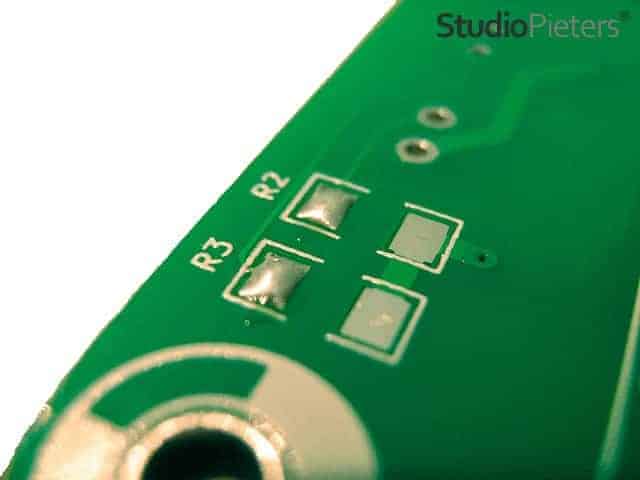
Resistors
For 5% precision SMD resistors usually are marked with their resistance values using three digits: two significant digits and a multiplier digit. These are quite often white lettering on a black background, but other colored backgrounds and lettering can be used.
The black or colored coating is usually only on one face of the device, the sides and other face simply being the uncoated, usually white ceramic substrate. The coated surface, with the resistive element beneath is normally positioned face up when the device is soldered to the board, although they can be seen in rare cases mounted with the uncoated underside face up, whereby the resistance value code is not visible.
For 1% precision SMD resistors, the code is used, as three digits would otherwise not convey enough information. This code consists of two digits and a letter: the digits denote the value’s position in the E96 sequence, while the letter indicates the multiplier.
Typical examples of resistance codes
102 = 10 00 = 1,000 Ω = 1 kΩ
0R2 = 0.2 Ω
684 = 68 0000 = 680,000 Ω = 680 kΩ
499X = 499 × 0.1 = 49.9 Ω
There is an online tool to translate codes to resistance values. Resistors are made in several types; a common types uses a ceramic substrate. Resistance values are available in several tolerances defined in EIA Decade Values Table :
E3, 50% tolerance (no longer used)
E6, 20% tolerance (now seldom used)
E12, 10% tolerance
E24, 5% tolerance
E48, 2% tolerance
E96, 1% tolerance
E192, 0.5, 0.25, 0.1% and tighter tolerances
Capacitors
Non-electrolytic capacitors are usually unmarked and the only reliable method of determining their value is removal from the circuit and subsequent measurement with a capacitance meter or impedance bridge. The materials used to fabricate the capacitors, such as nickel tantalate, possess different colours and these can give an approximate idea of the capacitance of the component.[citation needed]
Light grey body colour indicates a capacitance which is generally less than 100 pF.
Medium grey colour indicates a capacitance anywhere from 10 pF to 10 nF.
Light brown colour indicates a capacitance in a range from 1 nF to 100 nF.
Medium brown colour indicates a capacitance in a range from 10 nF to 1 μF.
Dark brown colour indicates a capacitance from 100 nF to 10 μF.
Dark grey colour indicates a capacitance in the μF range, generally 0.5 to 50 μF, or the device may be an inductor and the dark grey is the color of the ferrite bead. (An inductor will measure a low resistance to a multimeter on the resistance range whereas a capacitor, out of the circuit, will measure a near infinite resistance.)
Generally physical size is proportional to capacitance and (squared) voltage for the same dielectric. For example, a 100 nF 50 V capacitor may come in the same package as a 10 nF 150 V device.
SMD (non-electrolytic) capacitors, which are usually monolithic ceramic capacitors, exhibit the same body color on all four faces not covered by the end caps.
SMD electrolytic capacitors, usually tantalum capacitors, and film capacitors are marked like resistors, with two significant figures and a multiplier in units of picofarads or pF, (10−12 farad.)
Examples
104 = 100 nF = 100,000 pF
226 = 22 μF = 22,000,000 pF
The electrolytic capacitors are usually encapsulated in black or beige epoxy resin with flat metal connecting strips bent underneath. Some film or tantalum electrolytic types are unmarked and possess red, orange or blue body colors with complete end caps, not metal strips.
Placing A SMD Component
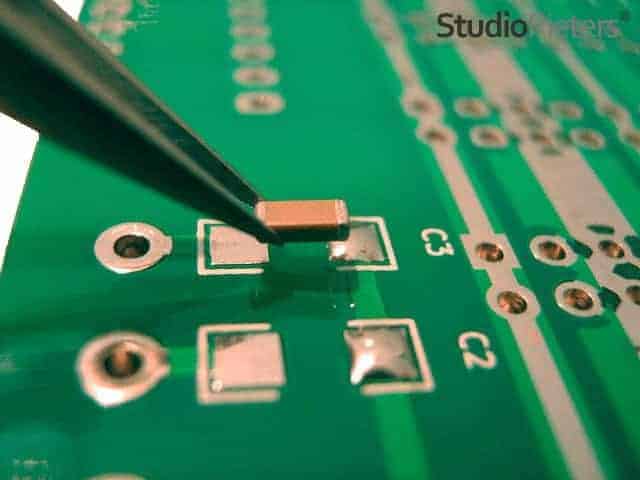
Apply a small amount of solder on one pad.
Then, with precision tweezers in one hand and your soldering iron in the other, place the component on the footprint.

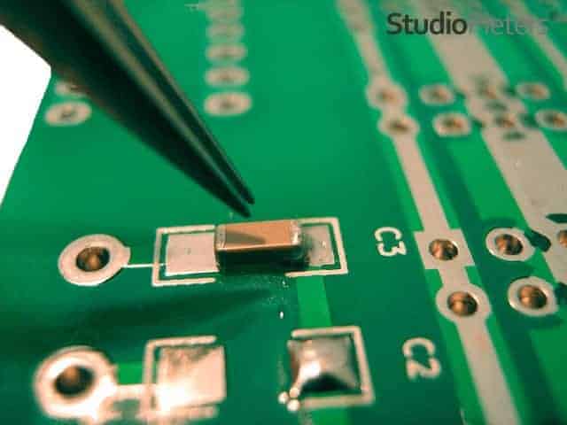
resent the component and re-flow the pad
When you’re ready, while maintaining the component with the tweezers, put the iron against the solder blob. The heat will melt the solder and, when cooling, the solder joint will keep the component in place. You have one pad done.
If needed, you can move the component again by melting the solder while dragging the component with the tweezers.
The component must be pushed against the PCB. If there’s an angle, you need to correct the position.
Now the component is stuck in place. You can solder the other side. (This one should be centered better!)
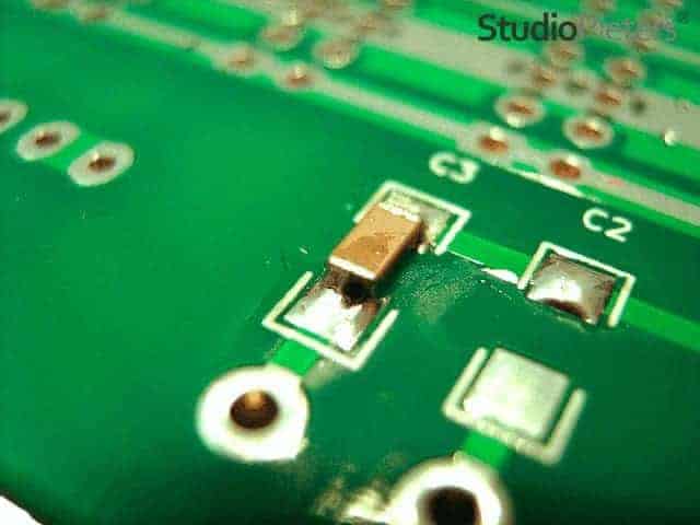
When the position is correct, it’s time to solder the second pad. This time, the technique is more traditional: the solder wire in one hand and the iron in the other, first apply the heat to the pad (PCB pad and component pad) and apply the smallest amount of solder.

DO YOU HAVE ANY QUESTIONS? LEAVE A COMMENT DOWN HERE.
REFERENCES
Surface-mount technology,(01 Okt 2017), Surface-mount technology (SMT) is a method for producing electronic circuits in which the components are mounted or placed directly onto the surface of printed circuit boards (PCBs). , https://en.wikipedia.org/wiki/Surface-mount_technology davidhaillant, (11 Feb 2017), How to Hand Solder SMD, https://www.davidhaillant.com/smd-soldering