In my previous blog I covered the hardware and software and part II here for my Raspberry Pi® – Powerunit® project. Now its time for the PCB Design.
KiCad
Although KiCad (pronounced ‘Kai-Cad’, not ‘Key-Cad’ like the thing that goes in a lock) is the new hotness when it comes to PCB design. The amazing growth of KiCad installations over the past few years is a long time coming. In development since 1992, KiCad has cemented itself as the premier Open Source PCB design suite, and since 2013 CERN© has been making contributions to the project.
Yes that’s right CERN© where they probe the fundamental structure of the particles that make up everything around us. And where they do so using the world’s largest and most complex scientific instruments.

More recently, the KiCad project has been showing off some amazing new features. These include 3D rendering of boards, interactive routing, push-and-shove, simulation, and dozens of other features that put it on a path to being on par with the top of the line EDA suites. Add in some great community contributions, and you have something really, really amazing. All of this is wrapped up in an Open Source license, free as in speech and beer.
You can download KiCad here.
Schematic
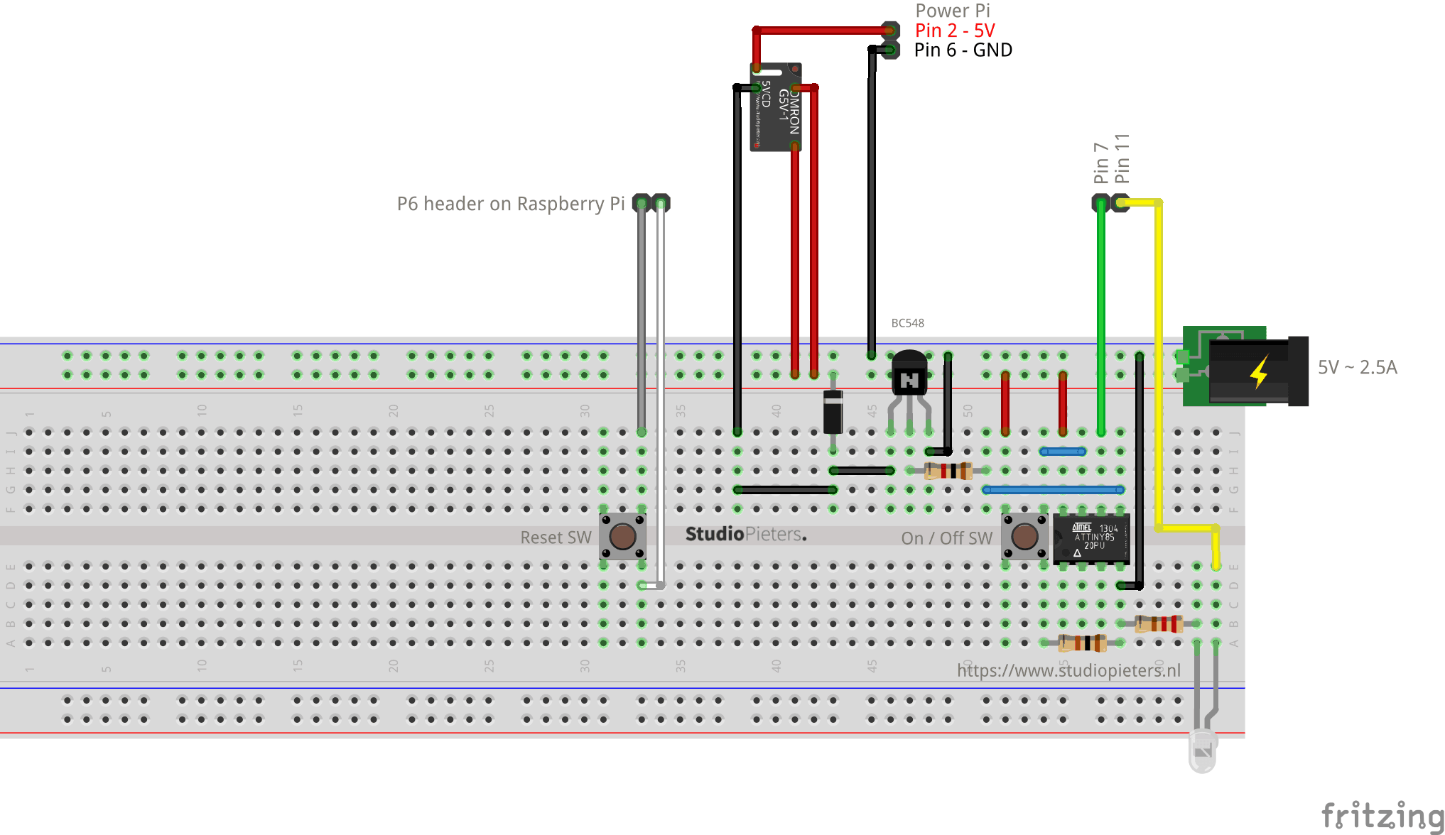
At first I need to design the schematic. So I open the fritzing scheme I made with the fritzing program.
I Also open the Kicad Program. And start a new project. After I don this I open the Eeschema – the schematic editor within Kicad. An introduction to the terminology of PCB design might be in order. A schematic is the abstract design file, showing the electrical connections between all the components in your circuit. The schematic is not sent to the fab house.
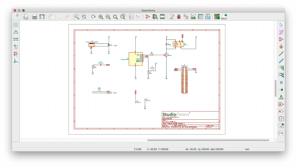
Don’t forget assigning footprints (the physical representation of components) to the parts in our schematic.With that, our schematic is done. We haven’t set any footprints up for each part, and we haven’t even started on the board yet.
From Schematic To Board
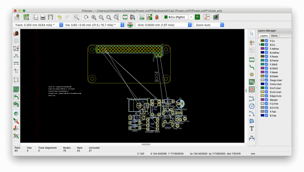
Now that the schematic has footprints associated to everything, it’s time to open up PCBnew, move parts around, and put some traces between parts. Do that. Oh, nothing shows up. Why is that? You need to generate a netlist in the schematic view, and import it in PCBnew. There’s a button with ‘NET’ written on it in both programs. Click those. Now, what do we get when the netlist is successfully imported into PCBnew? The worst mess you’ve ever seen in any sort of design program.
Putting everything In place
We end up with a gigantic mess on our hands. No worries, ‘M’ is the hotkey to move the parts around. You can also use the ‘Move Footprint’ mode to automatically place these parts.

Reference the PCB we designed for the introduction to this series and move some parts around until we get something resembling the board below. The relevant hotkeys are ‘M’ for move and ‘R’ for rotate.
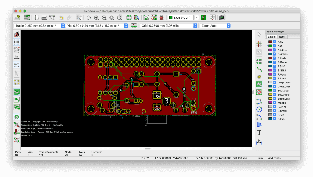
That’s it. We are technically done.
Although the KiCad beginner will struggle to wrap their heads around the interface, it will be one of the most powerful PCB design tools I’ll use in this series of posts. No other free (beer) program will give you 32 copper layers and unlimited routing space. Nothing else uses the cloud/GitHub like KiCad. It’s brilliant!

In my next blog about my Raspberry Pi® – Powerunit® project I’ll hope to have my PCB ready!
DO YOU HAVE ANY QUESTIONS? LEAVE A COMMENT DOWN HERE.
REFERENCE
Raspberry Pi® (2019), The Raspberry Pi is a tiny and affordable computer that you can use to learn programming through fun, practical projects, https://www.raspberrypi.orgPython™ (2019 )Python is a programming language that lets you work quickly and integrate systems more effectively, https://www.python.org/ PiSupply (DEC 5 2017), Pi-Supply-Switch, Pi Sup