In my previous Blog I made a ESP XXXX XX Programmer PCB in the KiCAd programme. Manufacturing of these PCB is the next step. In the last few years many inexpensive PCB Manufacturing services have popped up. It used to be that buying PCBs in hobby quantities was expensive and filled with gotchas. Now, places like Seeed Studio can send your PCBs to the inexpensive prototyping factory in Shenzhen China, and ship them anywhere in the world at great prices. You get two-sided PCBs, with the works, starting at $0.49 per 5x5cm PCB. Turnaround is a few days, worldwide shipping starts at $10. It’s a happy day for electronics hobbyists. Before you can place your order you need to generate so called Gerber files, needed for production of your PCB’s. Here I will explain how to generate these files.

How to generate Gerber and drill files for Manufacturing
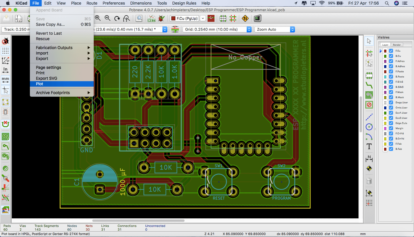
In KiCad, open your PCB design file and go to File -> Plot, or find the plot icon on the main interface.
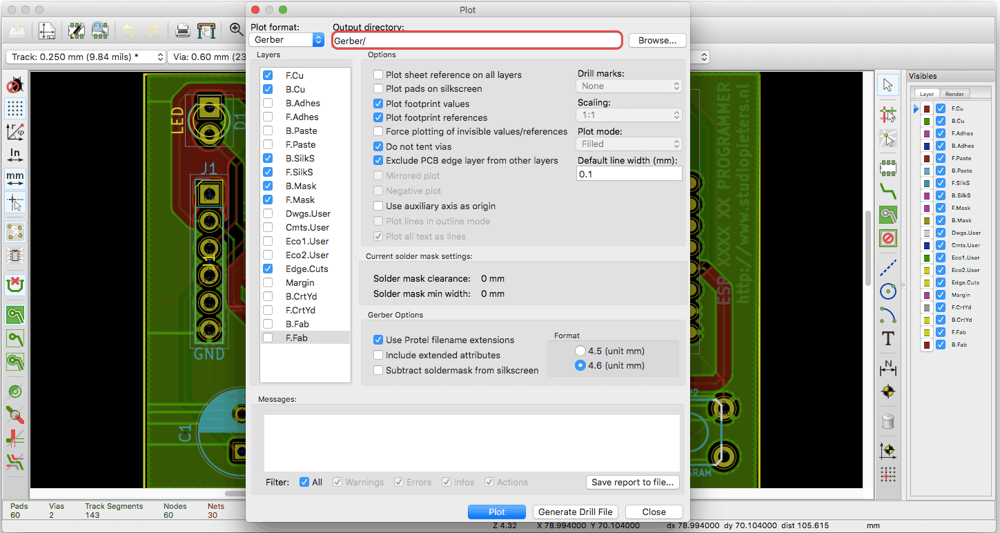
This will bring up the plot window. Select an output directory for your Gerber Files and select the following layers and options.
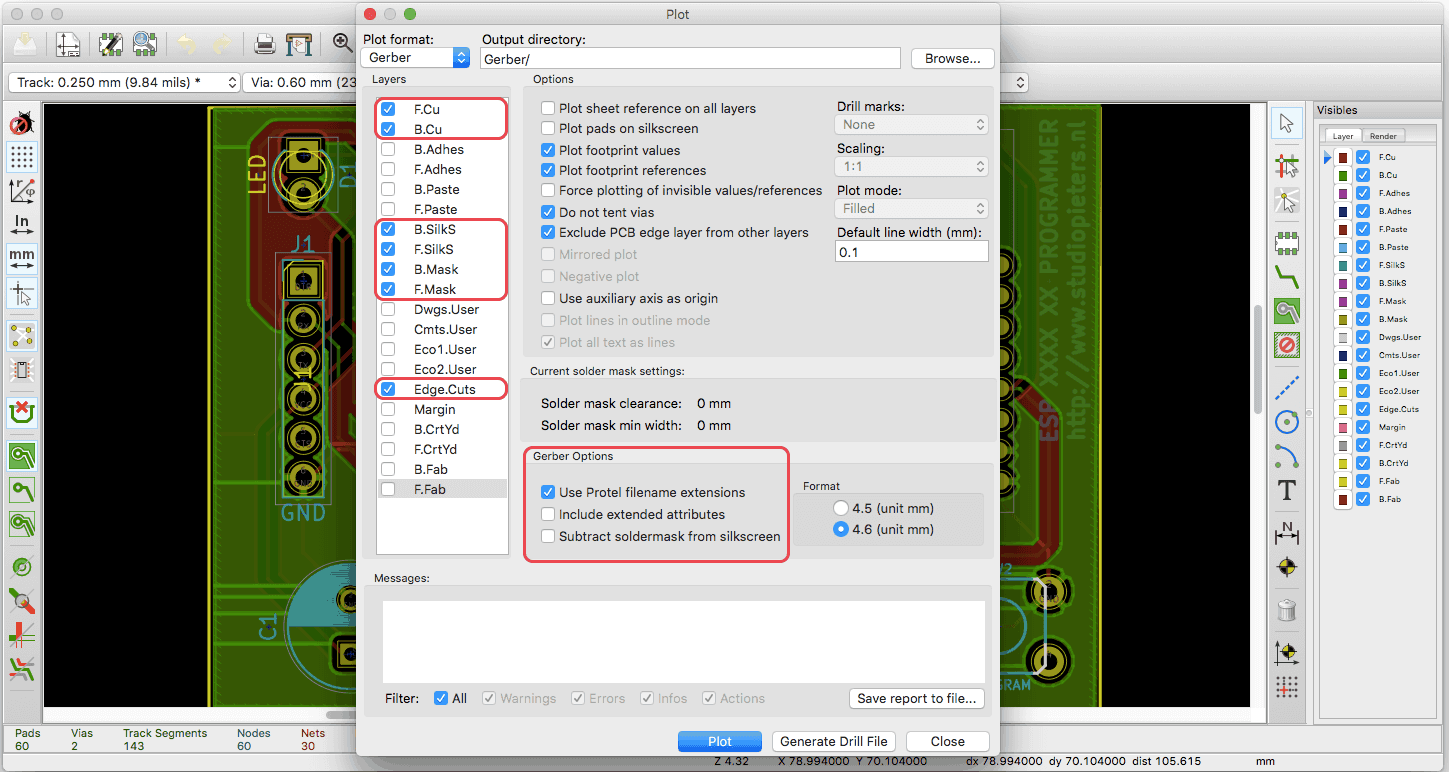
Please pay attention to the required layers, there should be 7 layers in total for typical two layer boards. If your boards are single or multi-layered, please select the necessary layers.
Please note that all mechanical elements such as cut-outs and v-cuts should be drawn in the Edge.Cuts layer.
If you need the paste layers for stencil orders, please check B.Paste and F.Paste as required.
Also, please ensure that you do not select the Include extended attributes option under Gerber Options. This will effectively convert the format of your Gerber files to X2, which not all our equipment supports.
Click Plot and confirm that all the Gerber files were generated successfully.
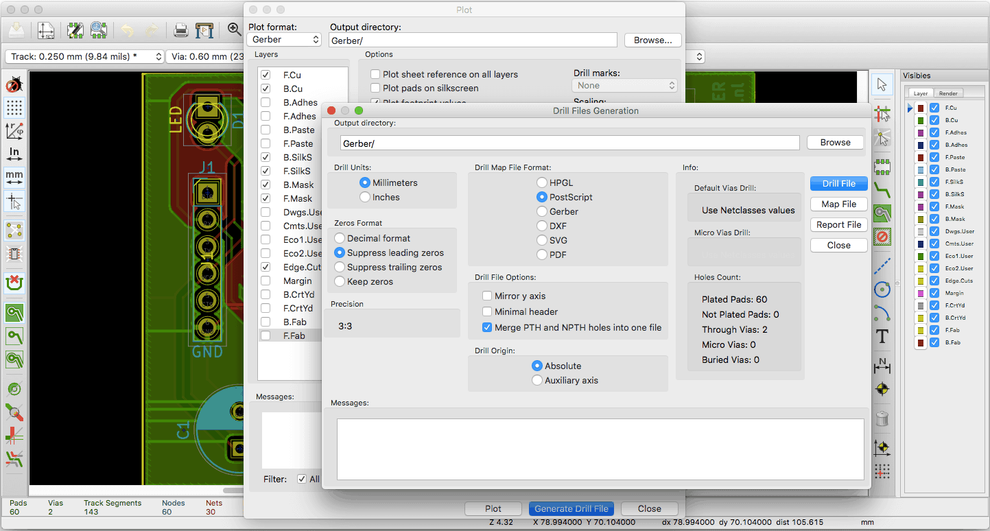
To generate the drill files, select the Generate Drill File button and this will open a new window. Click Drill File on the right and this is will export the drill file in Excellon format in your chosen directory.
We suggest you select the option to Merge PTH and NPTH holes into one file, otherwise KiCad will separate plated and non-plated holes into two drill files, and if one is missing, there will be holes missing on your boards.
Please check that you have all 8 (or 9) files then zip them into a .zip or .rar archive file. You can use this to place the order on the Seeed Fusion PCB order page. I would recommend that you give the files a quick check using the online Gerber Viewer before confirming the order.

Common Mistakes and Problems:
– Incorrect Format: Seeedstudio prefers the Gerber files to be in RS-274x format over X2 since all there equipment are compatible with RS-274x. However, in standard versions of KiCad, it is not obvious whether the files are being exported in X2 or RS-274x format. In the Plot window, by selecting Include extended attributes, this converts the files into X2 format and cannot be imported into our standard CAM software. Please ensure you do not select this option. In some versions of KiCad, this is mentioned but please ensure that all X2 options are unchecked.
– Missing mechanical holes: Since KiCad has the option to export the plated and non-plated drill holes separately, it is easy to forget to include them both in the archive. If the PTH drill file is missing, this is easy to catch. But if the NPTH drill file for the mechanical holes is missing, it can be easy to overlook. To avoid this issue we suggest selecting the Merge PTH and NPTH holes into one file option.
DO YOU HAVE ANY QUESTIONS? LEAVE A COMMENT DOWN HERE.
REFERENCE
Tech Explorations (Mar 16 2016), KiCAD LIKE A PRO, This course is designed to teach you how to use KiCad assuming no prior knowledge in PCB design. , http://kicad.txplore.com SEEED Studio (2008-2018), FUSION PCB MANUFACTURING, Fusion offers one stop prototyping services for PCB (Printed Circuit Board) , https://www.seeedstudio.io/fusion_pcb.html