For an upcoming project I need to improve the electrical characteristics of the PCB by increasing the width of the Ground and Vcc tracks. Let’s start with the track width. You can control the width of each track manually. The method involves creating custom track’s widths and then applying one of those to a new or existing track.

create custom track widths
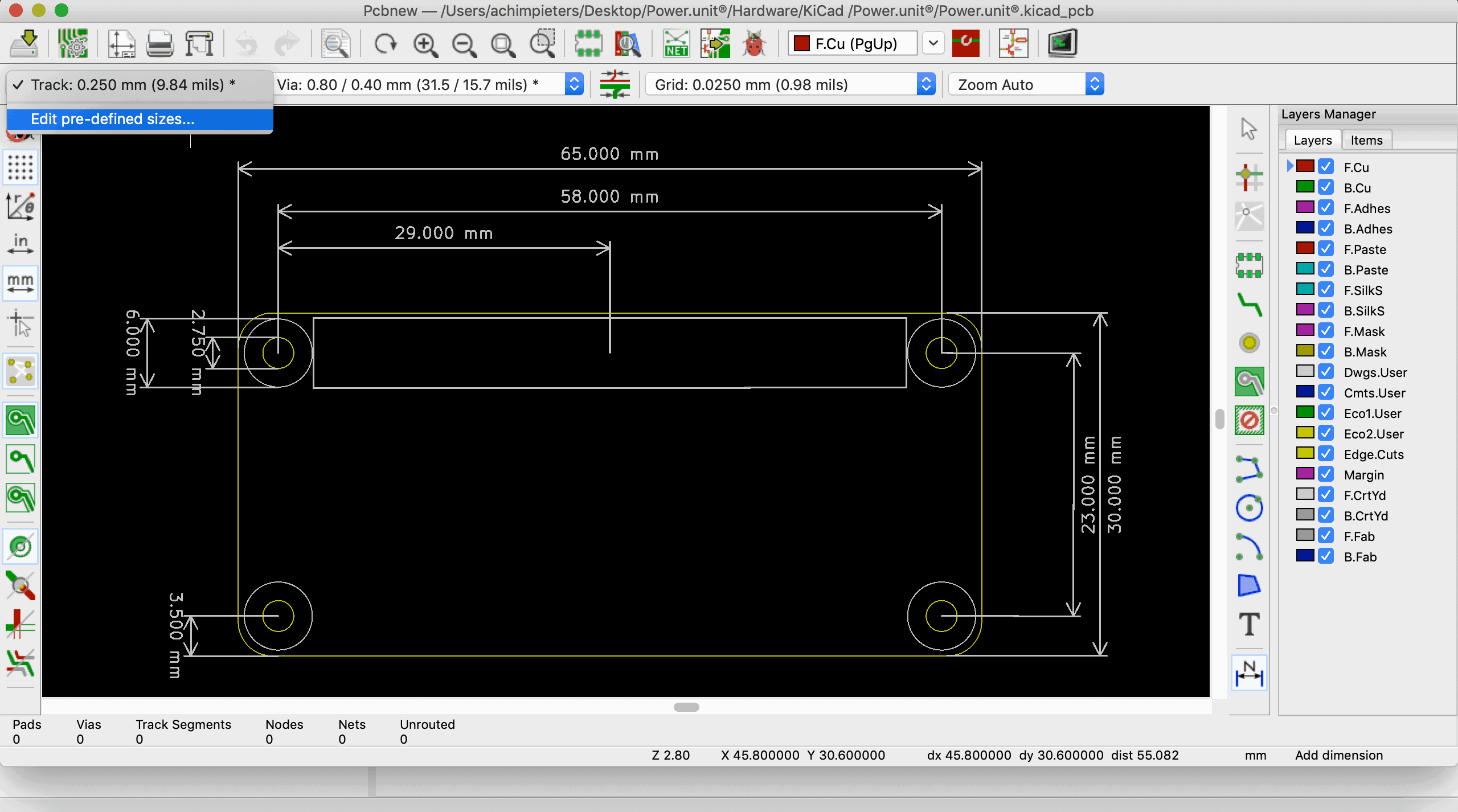
Let’s go ahead and add a few custom track widths that should cover 99% of your requirements. To do that, let’s go to design rules and check on the first option design rules. Click on the Track ↕ arrows and select Edit pre-defined sizes…. Once in the Board Setup click on the Track & via’s.
Notice, in the area of the window, two empty grids. On the right side you can see the Custom Via Sizes grid, and on the right side is the Custom Track Widths. We will populate these grids with our own values. Let’s work on the widths first. I looked up the manufacturing specifications for Seeed Studio (PCB manufacturing) and I found the typical widths that they support. I will use these numbers here. These numbers tend to be used across the industry, so chances are they will be right for many other fabricators.
Copy the custom widths to your Custom Track Widths grid:
| Width | |
| Track 1 | 0.1524 |
| Track 2 | 0.254 |
| Track 3 | 0.381 |
| Track 4 | 0.508 |
| Track 5 | 0.8128 |
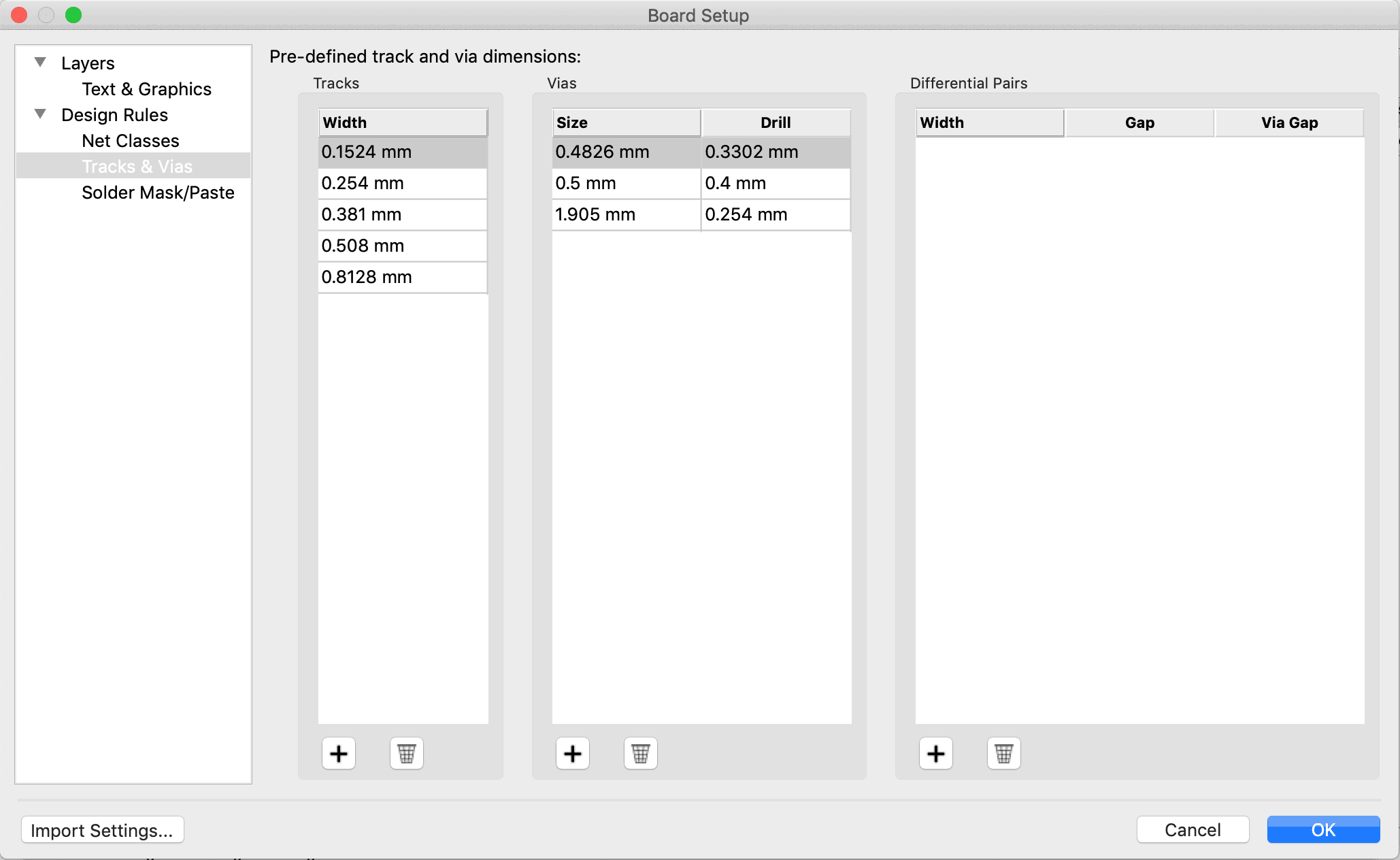 The custom track width sizes that work with Seeed Studio (PCB manufacturing) (and many other fabricators). Custom tracks 3, 4 and 5 are very large and unlikely I will ever use them, but we can include them for the sake of completeness.
custom via sizes
Even though, if you are not going to be using any via’s in your project, you maybe will in the next project. We might as well put them in here to have them ready to use later. Copy the values to your Custom Via Sizes grid.
| Diameter | Drill | |
| Via 1 | 0.4826 | 0.3302 |
| Via 2 | 0.5 | 0.4 |
| Via 3 | 1.905 | 0.254 |
The minimum allowed values must be at least equal to the smallest values in the two grids.
At the top left side of the window you will see the Design rules. None of the values in the two grids of this window can be smaller than the corresponding values in this group. I have entered the correct values to satisfy the minimum value rules in the Minimum Allowed Values group, so feel free to copy these values across to your Design Rules.
| Minimum Allowed Values: | |
| Min track width (mm): | 0.1524 |
| Min via diameter(mm): | 0.4 |
| Min via drill dia (mm): | 0.254 |
| Min uvia diameter (mm): | 0.2 |
| min uvia drill dia (mm): | 0.1 |
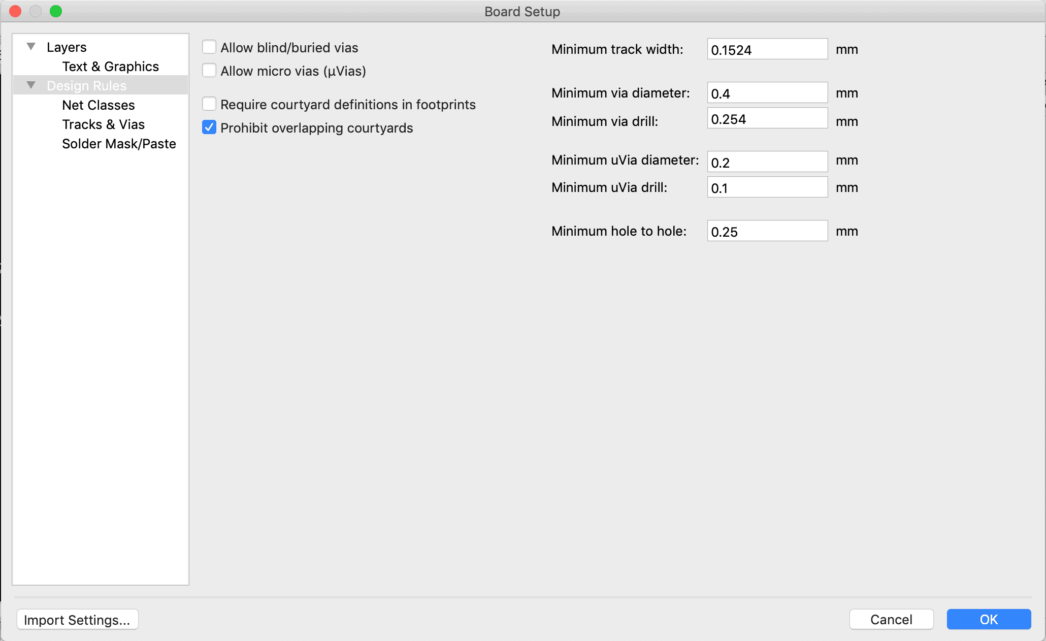 When you are finished, click on OK to commit the changes.

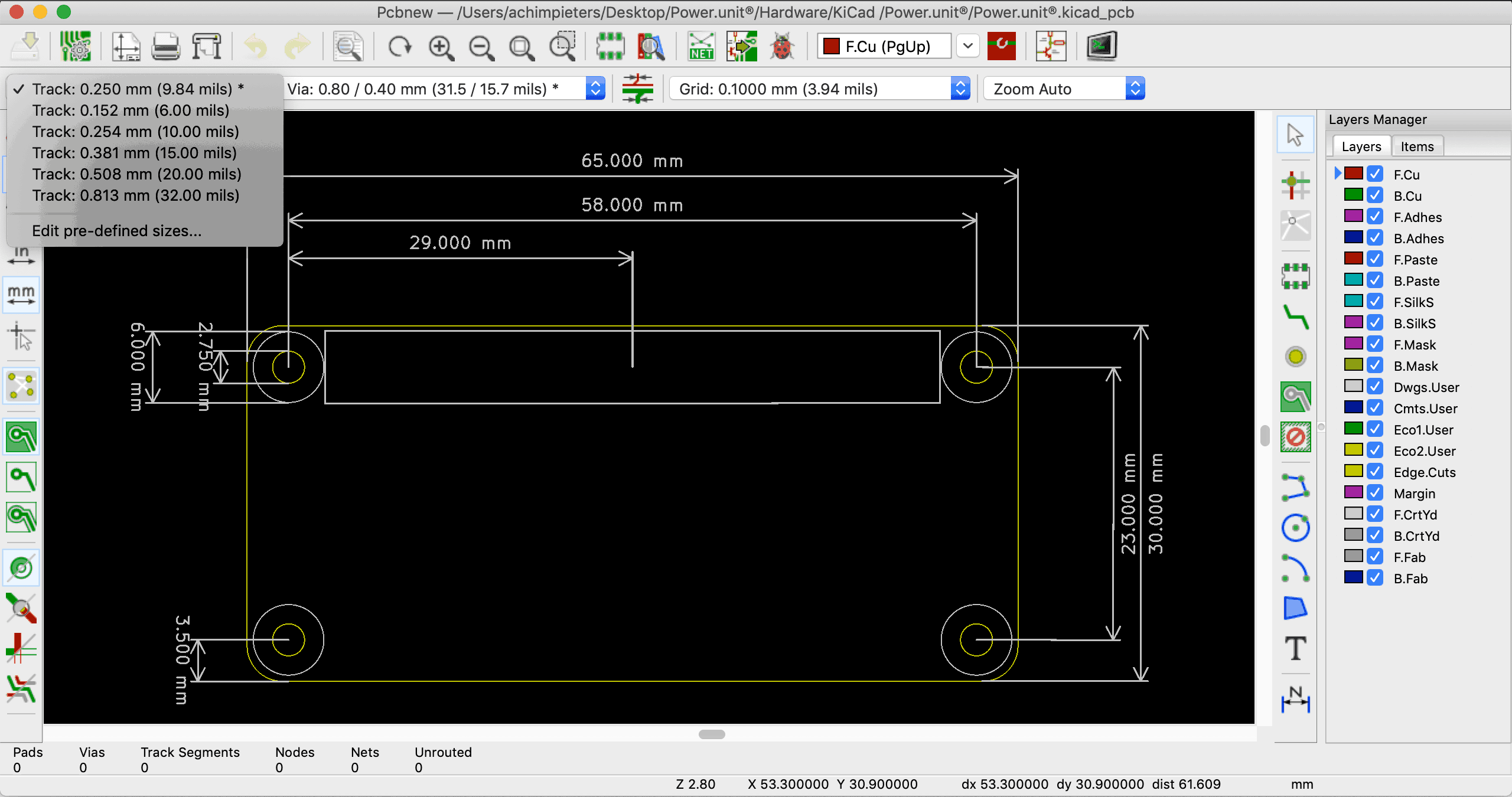
The custom track widths now appear in the width drop down menu.
You can now see that the values that we have just entered are available from the Track Width drop down menu.
DO YOU HAVE ANY QUESTIONS? LEAVE A COMMENT DOWN HERE.
REFERENCE
Tech Explorations (Mar 16 2016), KiCAD LIKE A PRO, This course is designed to teach you how to use KiCad assuming no prior knowledge in PCB design. , http://kicad.txplore.com SEEED Studio (2008-2018), FUSION PCB MANUFACTURING, Fusion offers one stop prototyping services for PCB (Printed Circuit Board) , https://www.seeedstudio.io/fusion_pcb.html