How to program a ATTiny I discussed in my previous blog here. But I want to go even smaller! In stead of using the “big” DIP IC housing I wan to use the smaller SOP IC housing. But then I realized how to program these tiny things, they don’t fit on a breadboard. But first some background information.

Integrated Circuit packaging types
DIP (Dual in-line packages)
DIP, short for Dual In-line Package, is the most common through-hole IC package you’ll encounter. These little chips have two parallel rows of pins extending perpendicularly out of a rectangular, black, plastic housing.
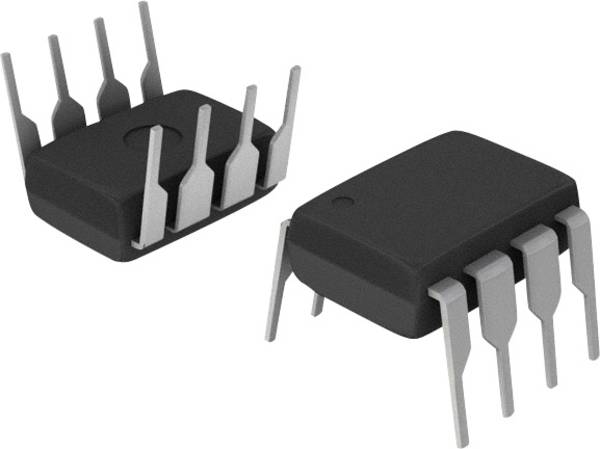
Each of the pins on a DIP IC are spaced by 0.1″ (2.54mm), which is a standard spacing and perfect for fitting into breadboards and other prototyping boards. The overall dimensions of a DIP package depend on its pin count, which may be anywhere from 4 to 64. The area between each row of pins is perfectly spaced to allow DIP IC’s to straddle the center area of a breadboard. This provides each of the pins its own row in the board, and it makes sure they don’t short to each other. Aside from being used in breadboards, DIP IC’s can also be soldered into PCB’s. They’re inserted into one side of the board and soldered into place on the other side. Sometimes, instead of soldering directly to the IC, it’s a good idea to socket the chip.
Small-Outline (SOP)
SO, Small-Outline IC (SOIC) packages are the surface-mount cousin of the DIP. It’s what you’d get if you bent all the pins on a DIP outward, and shrunk it down to size. With a steady hand, and a close eye, these packages are among the easiest SMD parts to hand solder. On SOIC packages, each pin is usually spaced by about 0.05″ (1.27mm) from the next.
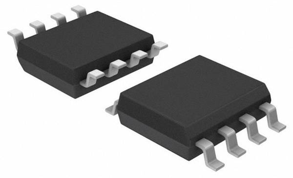
The SSOP (Shrink Small-Outline Package) is an even smaller version of SOIC packages. Other, similar IC packages include TSOP (Thin Small-Outline Package) and TSSOP (Thin-Shrink Small-Outline Package).
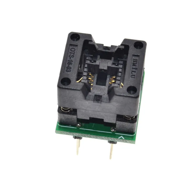
The solution
Because the SO, Small-Outline IC (SOIC) packages does not fit my breadboard and fond this Adapter for a programming module here on the Wavgat store on aliexpress.
ARDUINO NANO TO ATTINY85 CONNECTIONS
Let’s connect the necessary pins together on both boards.
1 x Arduino Nano (or any Arduino board will do)
1 x ATtiny85 (SOP)
1x Programming module
6 x Jumper Wires
1 x Electrolytic Capacitor – 10µF ~ 25V
We need to connect the MOSI, MISO and SCK pins of both boards together (refer to the IC pin out), and Digital Pin 10 of the Arduino Nano to P5 of the ATtiny85.
Connect the following (I am using an Arduino Nano, so you have to take note the necessary pins of the board you are using when using it as an ISP).
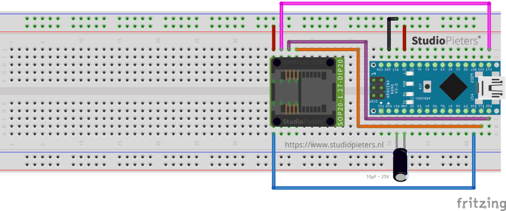
Add a 10uF capacitor between RESET and GND in Arduino. This is to avoid Arduino Nano from being auto reset when we upload the program to attiny85. If you are using a electrolytic capacitor make sure the anode goes in GND of Arduino Nano.
| Arduino Nano | ATTINY85 | |
| MOSI | Digital Pin 11 | PB0 (Chip Pin 5) |
| MISO | Digital Pin 12 | PB1 (Chip Pin 6) |
| SCL | Digital Pin 13 | PB2 (Chip Pin 7) |
| RESET | Digital Pin 10 | PB5 (Chip Pin 1) |
| VCC | VCC (5V) | VCC (Chip Pin 8) |
| GND | GND | GND (Any GND pin) |
There are two things we need to set up to successfully program the ATTiny85. For more information about programming a ATTiny go to my blog here.

FRITZING PART
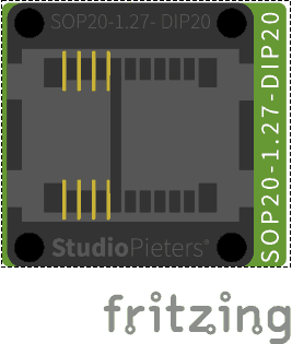
Because I always use the Fritzing app to illustrate the hardware setup of a new project, I need a new Fritzing part for future setup’s. So after some designing in illustrator this is the end result.
DOWNLOAD ALL FILES FOR THIS PROJECT ON GITHUB.

DO YOU HAVE ANY QUESTIONS? LEAVE A COMMENT DOWN HERE.