
Reference
Arduino UNO Q Pinout: 2 GB vs 4 GB
The Arduino UNO Q puts a Linux processor and a real-time microcontroller on one UNO-shaped board. This guide covers the 2 GB and 4 GB variants, every header pinout including JMISC and JMEDIA, the LEDs, power limits and the 1.8 V versus 3.3 V traps.
- Quad A53 + Cortex-M33
- Wi-Fi 5 + Bluetooth 5.1
- 2 or 4 GB RAM
- UNO form factor
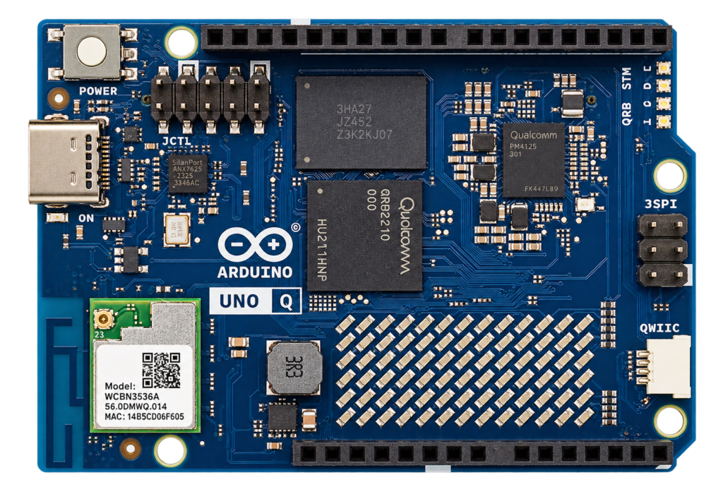
The Arduino UNO Q is a single-board computer in the classic UNO shape. It combines a Qualcomm Dragonwing QRB2210 processor running Debian Linux with an STMicroelectronics STM32U585 microcontroller running Arduino code on Zephyr. It comes in two variants, 2 GB and 4 GB, that differ only in memory and storage. This guide covers both, with the full header pinout, the power limits and the things that catch people out. Every number comes from Arduino’s own UNO Q user manual (SKU ABX00162-ABX00173, modified 21/10/2026).
Overview
Most boards on this site have one processor. The UNO Q has two, and they split the work: the Linux processor handles Wi-Fi, Bluetooth, USB-C and the camera and display lanes, the microcontroller handles the UNO headers, ADC, PWM, CAN and the LED matrix. The two talk through Bridge, Arduino’s RPC (remote procedure call) library: a sketch can call a service on the Linux side, and a Python program on Linux can call functions on the microcontroller. In Arduino App Lab, one “App” bundles a Python program, an Arduino sketch and optional Bricks (ready-made services such as AI models or web servers).


The data sheet lists Wi-Fi 5 (dual-band) and Bluetooth 5.1 on one shared module and no 802.15.4 radio. Only badges for what this exact board supports are shown.
| MPU (the Linux side) | MCU (the Arduino side) | |
|---|---|---|
| Chip | Qualcomm Dragonwing QRB2210 | STMicroelectronics STM32U585 |
| Cores | 4 x Arm Cortex-A53 at 2.0 GHz, 64-bit | Arm Cortex-M33, up to 160 MHz |
| Runs | Debian Linux | Arduino Core on Zephyr OS |
| Extras | Adreno 702 GPU at 845 MHz, dual camera ISPs | 2 MB flash, 786 kB SRAM |
| I/O voltage | 1.8 V | 3.3 V |
| Handles | Wi-Fi, Bluetooth, USB-C, camera, display | UNO headers, ADC, PWM, CAN, LED matrix |
2 GB or 4 GB?
Arduino sells two variants. Everything else is identical: same processors, same wireless module, same headers, same pinout.
| ABX00162 | ABX00173 | |
|---|---|---|
| RAM (LPDDR4X) | 2 GB | 4 GB |
| On-board storage (eMMC) | 16 GB | 32 GB |
| Processors, wireless, headers | Same | Same |
Which one should you buy?
- Pick the 4 GB variant if you want to use the board as a stand-alone computer. Arduino’s manual recommends it for running App Lab directly on the board (Single-Board Computer mode), “to ensure sufficient memory for stable operation and resource-intensive applications”. Also pick it for computer vision, AI models, or anything that keeps several services running at once.
- The 2 GB variant is the sensible choice when the board mostly drives hardware and runs a small Python program, with the code written on your own PC. That is my judgement, not a statement from Arduino.
- Memory is shared with the GPU. The Adreno GPU uses unified memory, so graphics work takes RAM from the same pool. The manual lists 1740 MB of available video memory but does not say for which variant, so treat it as an upper bound.
You cannot upgrade later
The RAM and the eMMC are soldered on. If you are unsure, the 4 GB variant is the safer choice, the 2 GB variant cannot be expanded.
Getting started
You develop in Arduino App Lab, either on your own computer (PC-hosted mode) or directly on the board (Single-Board Computer mode, SBC).
The first boot takes 20 to 30 seconds while Linux starts, and the LED matrix shows the boot logo during that time. Do not touch the matrix before it has finished, that can interfere with the microcontroller.
Hello World: blink the LED
The Blink LED example turns the red channel of a built-in RGB LED on for one second and off for one second. The LED is driven by the STM32U585 through the Arduino sketch. Every time you run an App, the sketch is compiled and the Python application starts on Linux, which can take up to a minute.
To blink an LED of your own, wire one with a resistor to D13 and use this sketch. Serial output appears in the Sketch tab of the App Lab console.
// Blink an external LED on D13 and print to the Sketch console in App Lab.
// LED + 330 ohm resistor from D13 to GND. D13 is 3.3 V logic.
void setup() {
  Serial.begin(115200);
  pinMode(13, OUTPUT);
}

void loop() {
  digitalWrite(13, HIGH);
  Serial.println("D13 high");
  delay(1000);
  digitalWrite(13, LOW);
  Serial.println("D13 low");
  delay(1000);
}
The App Lab steps follow Arduino’s manual. This sketch was not run on a board for this guide, so test it before relying on it.
Check that the App is running
The App Lab console has three tabs: Start-up (MCU compilation and Linux deployment), Main (Python) (the Python output) and Sketch (Microcontroller) (the serial output of the sketch). An App can start fine and still have runtime errors, so check the Python log. A sketch compile error aborts the launch.
Specifications
| Property | UNO Q |
|---|---|
| Wireless | Wi-Fi 5 (dual-band) and Bluetooth 5.1, shared antenna |
| USB-C | USB 3.1 with role switching, DisplayPort Alt Mode, power input |
| Video out (USB-C) | Full HD supported, 1280 x 720 optimal |
| Camera and display | 4-lane MIPI-CSI-2 and MIPI-DSI on JMEDIA (1.8 V) |
| LED matrix | 8 x 13 monochrome blue LEDs (104 pixels), driven by the MCU |
| Size | 68.58 x 53.34 mm, UNO form factor, bottom-side parts under 2 mm |
| Operating temperature | -10 to 60 degrees Celsius (ambient) |
| Power button | A long press (5 seconds or more) restarts Linux, it does not cut power |
Graphics and video
| API | Driver | Hardware support | Driver version |
|---|---|---|---|
| Desktop OpenGL | freedreno | not listed | 3.1 |
| OpenGL ES | freedreno | 3.1 | 3.1 |
| Vulkan | turnip | 1.1 | 1.0.318 |
| OpenCL | Mesa | 2.0 | 2.0 |
The GPU runs at 845 MHz, shares system RAM and has 64-bit addressing. Video encoding and decoding is reached through GStreamer (H.264, H.265 and VP9 decoding, H.264 and H.265 encoding) or other V4L2 frameworks. This pipeline from the manual decodes an H.264 file with hardware acceleration:
gst-launch-1.0 filesrc location=videos/xxxxx.mp4
  ! qtdemux name=demux demux.video_0 ! queue ! h264parse ! v4l2h264dec
  ! videoconvert ! autovideosink
The board measures 68.58 x 53.34 mm. Bottom-side parts stay below 2 mm so the board can stack onto carrier bases. The outline and hole pattern follow, and are compatible with, the UNO form factor. For a detailed drawing, use the CAD and STEP files that Arduino provides.
Pinout diagram
All five user headers on one page, with the function of every pin. JDIGITAL, JANALOG, JSPI and Qwiic belong to the 3.3 V microcontroller, JCTL belongs to the 1.8 V processor. The full tables follow below, and the 60-pin JMISC and JMEDIA headers for carrier boards come after them.

Drawn from the pin maps in Arduino’s UNO Q user manual (sections 9.3 to 9.7).
GPIO quick reference: JDIGITAL (D0 to D21)
The 18-pin digital header is all 3.3 V logic and belongs to the STM32U585. The “~” marks pins with PWM.
| Pin | Name | MCU pin | Functions | Notes |
|---|---|---|---|---|
| 1 | D0 | PB7 | USART1_RX, TIM4_CH2 | UART receive |
| 2 | D1 | PB6 | USART1_TX, TIM4_CH1 | UART transmit |
| 3 | D2 | PB3 | TIM2_CH2 | |
| 4 | ~D3 | PB0 | OPAMP2_OUTPUT, TIM3_CH3 | PWM. Not 5 V tolerant (3.6 V max) |
| 5 | D4 | PA12 | FDCAN1_TX, TIM1_ETR | CAN transmit |
| 6 | ~D5 | PA11 | FDCAN1_RX, TIM1_CH4 | PWM, CAN receive |
| 7 | ~D6 | PB1 | TIM3_CH4 | PWM |
| 8 | D7 | PB2 | TIM8_CH4N | |
| 9 | D8 | PB4 | TIM3_CH1 | |
| 10 | ~D9 | PB8 | TIM4_CH3 | PWM |
| 11 | ~D10 | PB9 | SPI2_SS, TIM4_CH4 | PWM, SPI chip select |
| 12 | ~D11 | PB15 | SPI2_MOSI, TIM1_CH3N | PWM, SPI MOSI |
| 13 | D12 | PB14 | SPI2_MISO, TIM1_CH2N | SPI MISO |
| 14 | D13 | PB13 | SPI2_SCK, TIM1_CH1N | SPI clock |
| 15 | GND | Ground | ||
| 16 | AREF | Analog reference | Not a GPIO | |
| 17 | D20 | PB11 | I2C2_SDA, TIM2_CH4 | I2C data |
| 18 | D21 | PB10 | I2C2_SCL, TIM2_CH3 | I2C clock |
Most JDIGITAL pins are 5 V tolerant as inputs, with one exception: D3 (PB0) is only 3.6 V tolerant. Never apply 5 V to it, in any mode.
GPIO quick reference: JANALOG (A0 to A5)
The 14-pin analog header carries the six analog inputs plus the power pins that shields expect on an UNO.
| Pin | Name | Net / MCU pin | Functions | Notes |
|---|---|---|---|---|
| 1 | BOOT | MCU_BOOT0 | Boot strap | |
| 2 | IOREF | PWR_3P3V | I/O voltage reference (3.3 V) | Output only |
| 3 | RESET | MCU_NRST | MCU reset | |
| 4 | +3V3 OUT | PWR_3P3V | 3.3 V supply | |
| 5 | +5V OUT | 5V_SYS | 5 V supply (diode-OR) | Power in or out |
| 6, 7 | GND | GND | Ground | |
| 8 | VIN IN | DC_IN | 7 to 24 V input | Power only |
| 9 | A0 / D14 | PA4 | ADC input, DAC0, TIM2_CH1 | Not 5 V tolerant |
| 10 | A1 / D15 | PA5 | ADC input, DAC1, TIM3_CH1 | Not 5 V tolerant |
| 11 | A2 / D16 | PA6 | ADC input, OPAMP2_INPUT+, TIM3_CH2 | |
| 12 | A3 / D17 | PA7 | ADC input, OPAMP2_INPUT- | |
| 13 | A4 / D18 | PC1 | ADC input, I2C3_SDA, LPTIM1_CH1 | |
| 14 | A5 / D19 | PC0 | ADC input, I2C3_SCL, LPTIM1_IN1 |
A0 and A1 are direct ADC inputs referenced to about 3.3 V. The absolute maximum on the pin is about 3.6 V, above that the MCU’s protection diodes start to conduct. When A4 and A5 are used as I2C3 (PC1 and PC0), use pull-ups to 3.3 V only.
JSPI, Qwiic and JCTL
JSPI (6 pins, 3.3 V)
| Pin | Name | Net |
|---|---|---|
| 1 | MISO | PC2 (SPI2_MISO) |
| 2 | +5V | 5V_SYS (power in or out) |
| 3 | SCK | PD1 (SPI2_SCK) |
| 4 | MOSI | PC3 (SPI2_MOSI) |
| 5 | RESET | MCU_NRST |
| 6 | GND | Ground |
The SPI pins are 5 V tolerant as inputs, while outputs drive 3.3 V, so add level shifting if you need a 5 V input threshold. Chip select comes from a GPIO on JDIGITAL or JMISC.
Qwiic (4 pins, 3.3 V)
| Pin | Name | Net |
|---|---|---|
| 1 | GND | Ground |
| 2 | +3V3 OUT | PWR_3P3V, supply for Qwiic devices |
| 3 | SDA | PD13 (I2C4_SDA) |
| 4 | SCL | PD12 (I2C4_SCL) |
The Qwiic connector is plug and play with Modulino nodes and third-party Qwiic sensors.
JCTL (10 pins, 1.8 V)
The control header belongs to the Linux processor, not the microcontroller, so it is 1.8 V.
| Pin | Name | Function |
|---|---|---|
| 1, 7 | GND | Ground |
| 2 | USB_BOOT | Boot strap (forced USB boot) |
| 3 | VOL_DOWN | GPIO_36 |
| 4 | SOC_SE4_TX | Console UART TX |
| 5 | VOL_UP | GPIO_96 |
| 6 | SOC_SE4_RX | Console UART RX |
| 8 | PMIC_RESET | PMIC reset |
| 9 | +1V8 OUT | 1.8 V reference |
| 10 | VBUS_DISABLE | Disables the VBUS power switch |
The SE4 UART is the system console. It is separate from the application UARTs and should not be reused for your own I/O.
Built-in LEDs
| LED | Driven by | Pins | Default |
|---|---|---|---|
| RGB LED 1 (D27301) | Linux | red:user GPIO_41, green:user GPIO_42, blue:user GPIO_60 | User controlled |
| RGB LED 2 (D27302) | Linux | red:panic GPIO_39, green:wlan GPIO_40, blue:bt GPIO_47 | System status, panic, WLAN, Bluetooth |
| RGB LED 3 (D27401) | MCU | PH10 red, PH11 green, PH12 blue | User controlled |
| RGB LED 4 (D27402) | MCU | PH13 red, PH14 green, PH15 blue | User controlled |
| Power LED (D27201) | Hardware | Tied to the 3.3 V rail | On whenever the board is powered |
The RGB LEDs are active low: they turn on when driven to logic 0. The two Linux LEDs are exposed through /sys/class/leds/ and use PWM at about 2 kHz.
JMISC header (60 pins, mixed voltage)
The 60-pin JMISC header on the underside is meant for carrier boards. It mixes 3.3 V microcontroller signals (parallel camera bus, SDMMC1 test pins, trace, I2C4, op-amp pins), analog audio and 1.8 V processor GPIO. The processor GPIO on this header are interface-dedicated, not general-purpose maker pins.
| Pin | Name | MCU pin | Domain | Notes |
|---|---|---|---|---|
| 1 | MCU_PSSI_D0 | PC6 | 3.3 V | PSSI data 0 |
| 2 | MCU_SDMMC1_CMD | PD2 | 3.3 V | SDMMC1 command / test |
| 3 | MCU_PSSI_D1 | PC7 | 3.3 V | PSSI data 1 |
| 4 | MCU_TRACE_CLK | PE2 | 3.3 V | Trace clock |
| 5 | MCU_PSSI_D2 | PC8 | 3.3 V | PSSI data 2 |
| 6 | MCU_TRACE_D0 | PE3 | 3.3 V | Trace data 0 |
| 7 | MCU_PSSI_D3 | PC9 | 3.3 V | PSSI data 3 |
| 8 | MCU_TRACE_D2 | PE5 | 3.3 V | Trace data 2 |
| 9 | MCU_PSSI_D4 | PE4 | 3.3 V | PSSI data 4 |
| 10 | MCU_TRACE_D3 | PE6 | 3.3 V | Trace data 3 |
| 11 | MCU_PSSI_D5 | PI4 | 3.3 V | PSSI data 5 |
| 12 | MCU_PE7 | PE7 | 3.3 V | GPIO |
| 13 | MCU_PSSI_D6 | PI6 | 3.3 V | PSSI data 6 |
| 14 | MCU_PE8 | PE8 | 3.3 V | GPIO |
| 15 | MCU_PSSI_D7 | PI7 | 3.3 V | PSSI data 7 |
| 16 | MCU_I2C4_SCL | PF14 | 3.3 V | I2C4 clock |
| 17 | MCU_PSSI_PDCK | PD9 | 3.3 V | PSSI clock |
| 18 | MCU_I2C4_SDA | PF15 | 3.3 V | I2C4 data |
| 19 | MCU_PSSI_RDY | PI5 | 3.3 V | PSSI ready |
| 20 | MCU_OPAMP1_VOUT | PA3 | Analog | OpAmp1 output |
| 21 | MCU_PSSI_DE | PD8 | 3.3 V | PSSI data enable |
| 22 | MCU_OPAMP1_VINP | PA0 | Analog | OpAmp1 positive input |
| 23 | MCU_MCO | PA8 | 3.3 V | MCU clock out |
| 24 | MCU_OPAMP1_VINM | PA1 | Analog | OpAmp1 negative input |
| 25 | MCU_CRS_SYNC | PA10 | 3.3 V | CRS sync |
| 26, 27, 35, 44, 58 | GND | Power | Ground | |
| 28 | EAR_P_R | Analog | Audio ear P_R | |
| 29 | MIC2_INP | Analog | Mic2 input + | |
| 30 | EAR_M_R | Analog | Audio ear M_R | |
| 31 | MIC2_INM | Analog | Mic2 input – | |
| 32 | LINEOUT_P | Analog | Line out + | |
| 33 | MIC2_BIAS | Analog | Mic2 bias | |
| 34 | LINEOUT_M | Analog | Line out – | |
| 36 | HPH_L | Analog | Headphone left | |
| 38 | HPH_R | Analog | Headphone right | |
| 40 | HPH_REF | Analog | Headphone reference | |
| 42 | HS_DET | Analog | Headset detect | |
| 37, 39, 41, 43 | SOC_GPIO_0, 1, 2, 3 (SE0) | 1.8 V | MPU GPIO | |
| 45, 47 | SOC_GPIO_86, 82 (SE0) | 1.8 V | MPU GPIO | |
| 46, 48 | SOC_GPIO_98, 99 | 1.8 V | MPU GPIO | |
| 49, 51 | SOC_GPIO_18, 28 | 1.8 V | MPU GPIO | |
| 50, 52 | SOC_GPIO_100, 101 | 1.8 V | MPU GPIO | |
| 53, 55 | +3V3 (OUT) | Power | 3.3 V power out | |
| 54, 56 | +5V_SYS (OUT) | Power | Power in or out, diode-OR | |
| 57 | +1V8 (IN) | Power | 1.8 V rail in | |
| 59 | VCOIN (IN) | Power | System voltage (PMIC RTC) | |
| 60 | VBAT (OUT) | Power | Reserved for system design and future features |
Check the voltage domain of every pin before you attach a carrier. MCU pins are 3.3 V, processor pins are 1.8 V and the audio pins are analog.
JMEDIA header (60 pins, camera and display)
JMEDIA carries the high-speed camera and display signals in the 1.8 V domain: one 4-lane MIPI-DSI display port (clock plus lanes 0 to 3) and two MIPI-CSI camera ports, CSI0 and CSI1 (a clock and four data lanes each). The lanes are differential D-PHY pairs, not general-purpose I/O. The other pins are ground and the control and power pins below.
| Pin | Name | Domain | Function |
|---|---|---|---|
| 16 | SOC_CAM_MCLK0 (GPIO_20) | 1.8 V MPU | Camera master clock 0 |
| 18 | SOC_CAM_MCLK1 (GPIO_21) | 1.8 V MPU | Camera master clock 1 |
| 22 | CCI_I2C_SDA1 (GPIO_29) | 1.8 V MPU | Camera control I2C data 1 |
| 24 | CCI_I2C_SCL1 (GPIO_30) | 1.8 V MPU | Camera control I2C clock 1 |
| 51 | CCI_I2C_SCL0 (GPIO_23) | 1.8 V MPU | Camera control I2C clock 0 |
| 53 | CCI_I2C_SDA0 (GPIO_22) | 1.8 V MPU | Camera control I2C data 0 |
| 57, 59 | VIN (IN) | Power | 7 to 24 V input, power only |
| 58, 60 | +3V3 (OUT) | Power | 3.3 V power out |
The camera control I2C lines and camera clocks are reserved in the Linux device tree and must not be used as general-purpose I/O. VIN on JMEDIA is the raw 7 to 24 V input, power only. The MIPI-DSI signal is shared with the USB-C DisplayPort output, so only one display output is active at a time.
Powering the board
| Source | Voltage | Maximum current | Where |
|---|---|---|---|
| USB-C VBUS | 5 V (4.5 to 5.5 V) | Up to 3 A | USB-C connector |
| VIN (DC in) | 7 to 24 V | Not stated | JMEDIA and JANALOG (VIN) |
| 5 V pin (5V_SYS) | 5 V | Up to 3 A | JANALOG, JMISC, JSPI |
USB-C and the 5 V output of the 7 to 24 V buck converter are combined with diodes onto one 5 V bus (5V_SYS). From it the board derives 3.8 V, then 3.3 V, and the power management chip makes the 1.8 V rail. The 3.3 V rail may range from 3.1 to 3.5 V.
The board only asks USB Power Delivery for 5 V at 3 A, it never negotiates a higher voltage, so use a supply and cable that really deliver 3 A. A weak supply can show up as resets or dropped Wi-Fi during short load peaks such as wireless bursts or display initialization.
Safety notes
Before you wire anything up
Do not apply reverse voltage to DC in: the board was tested at -24 V, but it is only specified for the correct polarity. Never put 5 V on D3, A0 or A1, and no more than about 3.6 V on any analog pin. Check the voltage domain of every JMISC and JCTL pin, processor lines are 1.8 V. Do not reuse the reserved lines: the SE4 console UART, the camera control I2C and the MI2S0 audio bus are reserved in the Linux device tree. Keep 20 cm between the device and your body while it transmits, and note that the 5 GHz band can be restricted in some countries.
- Peripherals in SBC mode need a powered dongle. Use a USB-C dongle with external power delivery for keyboards, mice and cameras. While DisplayPort Alt Mode is active, USB data speed is reduced.
- While an App runs, USB can be busy. Stop the App or unplug the board before using external command-line tools over USB.
- The power button reboots Linux. A long press can interrupt a running App, save your work first.
- One display output at a time. USB-C DisplayPort and the JMEDIA display connector share one signal.
Conclusion
The UNO Q is two computers on one UNO-shaped board: a real-time microcontroller with the familiar UNO pins, and a Linux processor with Wi-Fi, USB and camera lanes. Choose the 4 GB variant for stand-alone and AI work, the 2 GB variant when it mainly drives hardware. A real build that uses it as the brain is the micro-Duck robot, see Part 2: the hardware for the parts list. For a Wi-Fi microcontroller without Linux, compare the XIAO ESP32S3 or the ESP32-WROOM-32D.
Source: Arduino UNO Q User Manual, SKU ABX00162-ABX00173, docs.arduino.cc, modified 21/10/2026. Check it for changes, this board is new.
Related
 Reference
SHT40 / SHT41 Temperature and Humidity Sensor Complete Guide
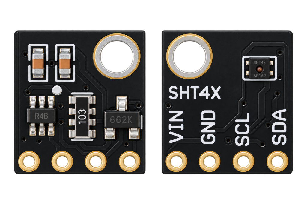
Sensirion's fourth-generation SHT4x sensors trade the SHT3x series' heater-based self-test for an ultra-low idle power budget and a slightly tighter accuracy spec. This guide covers wiring an SHT40 or SHT41 to an ESP32, real I2C addressing, and which SHT generation actually makes sense for a new project.
Read more
 Reference
NodeMCU-ESP32-C2 Pinout
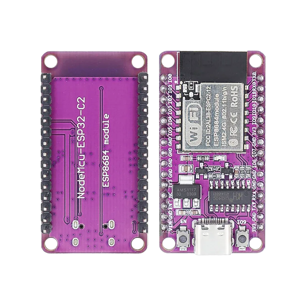
The complete pin reference for the NodeMCU-ESP32-C2: an ESP8684-WROOM-02 board with a USB-C port and CH340C, 13 usable GPIOs, Wi-Fi and Bluetooth LE.
Read more
 Reference
AI-C3 Pinout
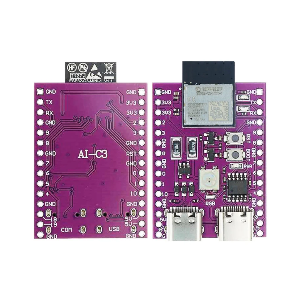
The complete pin reference for the AI-C3: a compact ESP32-C3-MINI-1 board with two USB-C ports, an RGB LED and 15 GPIOs.
Read more
More guides
Keep building.
From ESP32 HomeKit accessories to Arduino and ATtiny reference guides, there’s more where this came from.
All guides