Track width is one of the most critical factors of any printed circuit board (PCB) design. Anyone who has a good knowledge of track design will at some point face the challenge of determining the correct track width. Inexperienced designers tend to use the standard gauge given in the PCB layout software. And this can work to some extent. Those familiar with electronics would probably look at the standard width and intuitively know that it is too narrow for some tracks, especially for power and ground connections. You might bump it up a bit to something that “feels right” but don’t know how to scientifically set the right widths in your design.

Track width
Let’s start with the basics; A PCB trace is a thin line of conductive copper placed on a non-conductive or insulated base material that carries the signal and current to the entire circuit. A copper track has a certain width, which we call Track width, and has a certain height or thickness.
Usually the PCB thickness of this copper layer is fixed and the specifications of the PCB manufacturing company determine this. You measure PCB thickness in ounces per square foot in the United States. For typical PCB’s, the most common copper thickness is 35 µm, which equates to 1 oz/SQR ft (we would say 1 oz (approx. 38 g) of copper).
So in our design we only have control over the width of the tracks. For most manufacturers, the minimum track width should be 6mil or 0.152 mm. This limitation stems from their manufacturing (etching) processes and the intended yield. But to have some tolerance, we generally use 10-12 mil or 0.254-0.3 mm traces.
NOTE: FREE Download at the bottom of this article.
| Mil | Millimeter |
| .004mil | 0.1016 |
| .006mil | 0.15240000000000001 |
| .008mil | 0.20319999999999999 |
| .010mil | 0.2540 |
| .012mil | 0.30480000000000002 |
| .014mil | 0.35560000000000003 |
| .016mil | 0.40639999999999998 |
| .018mil | 0.4572 |
| .020mil | 0.5080 |
| .022mil | 0.55879999999999996 |
| .024mil | 0.60960000000000003 |
| .026mil | 0.6604 |
| .028mil | 0.71120000000000005 |
| .030mil | 0.7620 |
| .032mil | 0.81279999999999997 |
| .034mil | 0.8636 |
| .036mil | 0.91439999999999999 |
| .038mil | 0.96519999999999995 |
| .040mil | 1.0160 |
| .042mil | 1.0668 |
| .044mil | 1.1175999999999999 |
| .046mil | 1.1684000000000001 |
| .048mil | 1.2192000000000001 |
| .050mil | 1.2700 |

What Factors Are Essential for Track width?
To understand why different track widths matter, we must first understand their difference in a circuit. In a standard PCB, there are two main types of traces: signal traces and current traces.
Signal Traces
Signal traces are traces that transmit certain data. In digital or analogue signals, having different track widths generally doesn’t matter much in simple PCB designs, but is vital in RF/analogue and high-speed digital designs. In this type of design, track impedance is an essential consideration, as track width and impedance have an inverse relationship. We’ll talk about that in the Impedance section below. We’ll talk about that in the Impedance section below.
Power Traces
On the other hand, current traces require a little more attention because these traces are responsible for carrying current to each of the components in the circuit. There are two reasons for using different gauges in a PCB design.
1. Current Carrying Capacity
The current carrying capacity is the first and most obvious reason. Why? The relationship between the width of the conductor and the current capacity is simple. The cross-sectional area of a track and the allowable temperature rise determine how much current a track can carry. The cross-section of the track is also directly proportional to the copper thickness and track width.

As we increase the current flowing through a particular track, so does the temperature. The track has to do with that temperature rise. An easy way to ensure this is to increase the width of that track.

The IPC-2152 standards are the starting point for determining track widths. These standards use empirical data to generate the tables for calculating current limits for a given temperature rise. Working with a PCB track gauge versus the current table is excellent for evaluating your PCB track width/cross-sectional area. With this table, you can effectively determine an upper limit for the allowed flow in your traces. Given the infinite variables in PCB stack, you need to analyse the PCB using simulation to accurately measure the current density and temperature rise. But for most typical boards, the IPC tables are good enough.
Here’s a chart with different gauges and corresponding current values, limiting your temperature rise to 10 °C with a copper weight of 1 oz (ca. 38 g)/square foot. This chart should give you an idea of the most appropriate track gauge in your PCB design.
| Current / Ampère | Track width (mil) | Track width (mm) |
| 1 | .010mil | 0.2540 |
| 2 | .030mil | 0.7620 |
| 3 | .050mil | 1.2700 |
| 4 | .080mil | 2.0320 |
| 5 | .110mil | 2.7940 |
| 6 | .150mil | 3.8100 |
| 7 | .180mil | 4.5720 |
| 8 | .220mil | 5.5880 |
| 9 | .260mil | 6.6040 |
| 10 | .300mil | 7.6200 |
Several online tools can calculate the track width required to carry the rated current while keeping the track temperature below a specified limit. Actual results may vary depending on application and conditions.

2. Trace Impedance
Specific spacing and impedance may be required for high speed circuits to minimize crosstalk, coupling, and reflections. You need to calculate sensitive data lines, such as RF/analogue traces and high-speed traces. For high-frequency signals such as GHz bands, PCB traces do not work as simple connections.
Each copper trace has a certain series inductance and internal resistance, which are easily overlooked for simple low-speed designs. But in high-speed designs, the inductance of traces and the roughness of the copper surface with the skin effect will increase and likely affect the performance of the board. In addition, each signal trace contains a capacitance value between the return path and other nearby traces.
Track width and Signal Reflection
Signal reflection is an essential problem in designing high-performance electronic circuits. The phenomenon where part of the transmitted signal reflects to the source is called signal reflection, and signal reflection is undesirable because it causes signal distortion and oscillations.
Signal reflection in PCBs largely depends on the shape and route of traces. Trace discontinuities come into play when a trace changes direction, shape, or interfaces with a component. For example, if a track bends at an angle of 90 degrees, the track width changes significantly. At the point of bending, the track width is 1,414 times larger than the actual track width. This change in track width leads to a change in impedance and thus causes signal reflection. Professional PCB designers are aware of such issues and therefore avoid sharp bends and uneven track widths.

If left unattended, these factors can significantly degrade the overall performance of the system, as the impedance will differ at different points in the signal path. Trace coupling, especially when signals cross-plane junctions and cavities, causes crosstalk.

Considerations
Keep Traces Short
Every conductive material has a specific resistance. Therefore, the track resistance increases as the track becomes longer or narrower. When current flows through the track, it leads to a higher power loss due to Joule heating. Since the wasted power is converted to heat, the life of the board is shortened. Therefore, it is essential to keep tracks with higher currents as short as possible, to avoid blistering, delamination or worse – fire!
Isolate Sensitive Components From Heat Source
Electronic components such as voltage reference IC’s, analogue to digital converters and operational amplifiers are sensitive to temperature changes. Their output can affect when such components are exposed to heat. Therefore, these components must be thermally insulated from the heat sources. This can be achieved by creating recesses in the circuit board and installing thermal relief connections such as heat sinks.
Remove Solder Mask
To increase the current flowing through a trace, you can remove the solder mask, which exposes the bare copper traces. Then you can add another solder on the track, which will increase the thickness and reduce the resistance. This process allows more current to flow through the tracks without increasing the track width or additional copper thickness. This technique is common in power supplies and power amplifier designs.
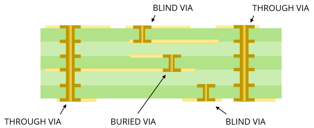
Use Same Net Tracks on Multiple Layers of the PCB
If there is no room to increase a certain track width on a single layer, you can route the track on multiple layers and use via’s to sew the tracks in different layers. This process will increase the current carrying capacity as the total surface area increases.

Use Internal Layers for High Current Paths
For more advanced and compact designs, multilayer PCBs are more suitable. Multilayer PCBs offer the benefits of higher board density, smaller size and improved reliability.
In multilayer PCB’s, designers use surface and internal traces differently depending on design and performance considerations. You can usually find traces carrying current signals on the surface due to heat ventilation requirements. Higher currents flow through the current signal traces, increasing their temperature. Internal PCB layers can trap heat and lead to thermal breakdown of power traces. For this reason, tracks carrying power signals are located on the surface layer.
Unlike the current signals, the traces carrying data signals are located on the internal layers. This placement reduces noise and protects against interference. Ambient signals from mobile phones, motors and power lines contribute to the signal noise. The exposed outer surface of the printed circuit board acts like an antenna and is therefore more sensitive to ambient noise. However, the internal copper layers are protected from this interference by the external copper layers. For this reason, the traces carrying critical data signals are always on the inner PCB layers.
Considerations
Trace Length and Spacing
Match the lengths of two differential tracks as closely as possible. The tolerance to match a signal and its complement depends on the data rate and the link rise time. For example, DDR4 signals clocked at 2400 MHz would match in length to inside. The result can be poor communication between devices. A standard specification for differential pair routing is 90 Ohm matched impedance. To achieve this specification, you need to optimize the track width and spacing.
Ground-Filled Traces and Planes:
Circuits that contain sensitive components, such as wireless chips or antennas, may need some extra protection from outside noise. You can minimize the need for additional protection through embedded ground via’s between tracks that can significantly reduce coupling, picked up by nearby tracks or aircraft, and off-board signals creeping into the edge of the board.
The size and shape of the copper trace on a PCB has a direct impact on the size, cost, and performance of the printed circuit board. In this context, the track width of a PCB is of enormous importance. Tracks intended to provide power signals must be wider due to higher power requirements. The track width of the PCB is inversely proportional to the track impedance. The following equation calculates the track impedance:

Where:
ρ = resistivity of copper | α = temperature coefficient of copper | T = trace thickness
W = Track width | L = trace length | t = temperature
Apart from the track width, the shape of the track affects the signal reflection. Asymmetric track dimensions and sharp bends give rise to signal reflection, which leads to signal distortion. In multi-layer PCBs, current signal traces are usually placed on the surface layer for improved heat ventilation. On the other hand, data signal traces are placed on the internal layers to protect against EMI and ambient noise.

In high-speed PCBs, reduction of crosstalk and EMI is an important consideration. For this reason, these PCBs often use differential pair signalling instead of single-ended signalling. In differential pair signalling, two tracks are used to carry a single signal. The differential pair signals are 180o out of phase, eliminating the crosstalk and noise.
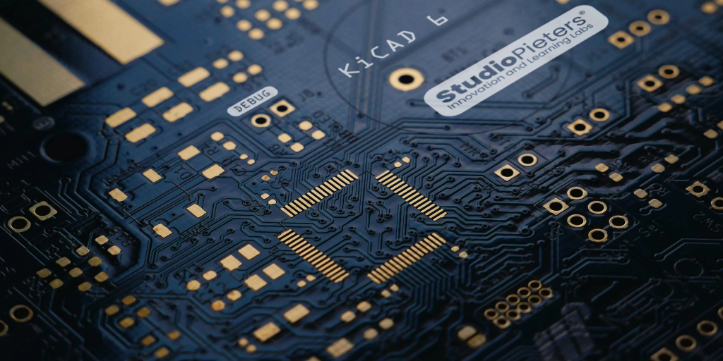
KiCAD 6
This article aims to educate you on the importance of selecting the correct gauges when designing PCBs. Track width is an essential parameter in PCB design and therefore should be chosen after careful calculations and estimates. Novice designers often err when selecting standard track widths, sometimes leading to inferior performance and even track damage. Read this article to learn how to improve your PCB design workflow with KiCAD 6.

Free Downloads
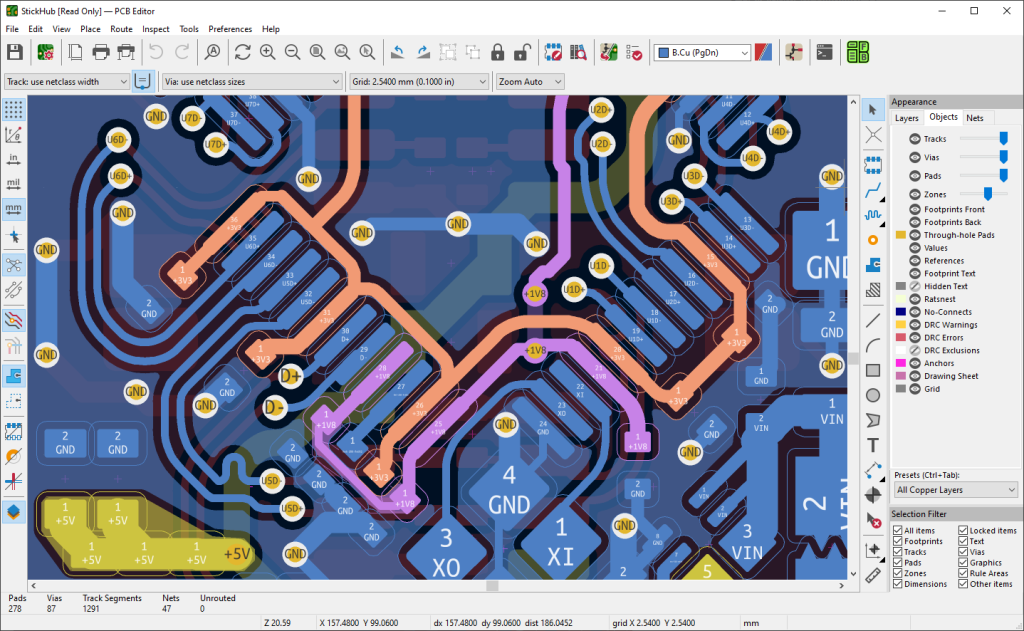
KiCAD 6
KiCad 6 EDA. A Cross Platform and Open Source Electronics Design Automation Suite.
KiCAD Track width settings.
Import all track settings automatically.
How to use: Download the files. Open your new project. Open your PCB file. Go to file, board setup. Then go to Design rules, Pre-defines Sizes. At the bottom, select Import settings from another board. Select Predefined track and via dimensions. Point to the folder where you put the files. And then import settings.
Reference
Seeedstudio, PCB Fabrication, https://support.seeedstudio.com/knowledgebase/articles/447362-fusion-pcb-specification autodesk, blog, https://www.autodesk.com/products/fusion-360/blog/trace-width