SMT / SMD Component Packages: sizes, dimensions, details it’s a whole world on itself. When you are looking for the right component you also need to decide witch package you will use. In my case as small as possible, but also I need to be able to solder it myself to my PCB.

SMD Component Packages
What is SMT / SMD Component Packages (Surface Mount Technology), Quad flat pack, QFP Ball grid array, BGA Plastic leaded chip carrier, PLCC. Surface mount technology, SMT components come in a variety of packages. There a several common sizes that are used and this enables the manufacturing pick and place machines to be set up to accommodate these sizes.
There has been a growing trend for small package sizes of most components. This has resulted from general improvements in technology and lower supply voltages for microprocessors and many digital ICs, again as a result of technology moving forwards. Additionally there is a variety of different SMT packages for integrated circuits dependent upon the level of interconnectivity required, the technology being used and a variety of other factors.
JEDEC SMT package standards
Industry standards are used to provide a large degree of conformity across the industry. Accordingly the sizes of most SMT / SMD Component Packages (Surface Mount Technology) conform to industry standards like the JEDEC specifications. Obviously different SMT packages are used for different types of components, but the fact that there are standards enables activities such as printed circuit board design to be simplified as standard pad sizes and outlines can be prepared and used.
Additionally the use of standard size packages simplifies the manufacture because pick and place machines can use standard feed for the SMT components, considerably simplifying the manufacturing process and saving costs. The different SMT packages can be categorised by the type of component, and there are standard packages for each.
Passive rectangular components
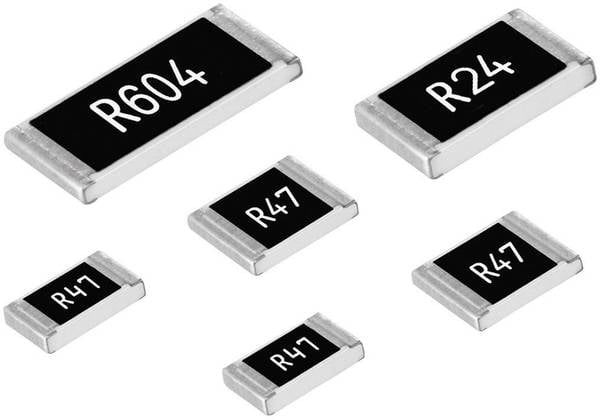
Passive surface mount devices are mainly comprised of resistors and capacitors. There are several different standard sizes which have been reduced as technology has enabled smaller components to be manufactured and used It will be seen that the devices size names are derived from their measurements in inches.
| Common Passive SMD Package Details | ||
|---|---|---|
| SMD Package type | Dimensions mm | Dimensions inches |
| 1812 | 4.6 x 3.0 | 0.18 x 0.12 |
| 1206 | 3.0 x 1.5 | 0.12 x 0.06 |
| 0805 | 2.0 x 1.3 | 0.08 x 0.05 |
| 0603 | 1.5 x 0.8 | 0.06 x 0.03 |
| 0402 | 1.0 x 0.5 | 0.04 x 0.02 |
| 0201 | 0.6 x 0.3 | 0.02 x 0.01 |
Of these sizes, the 1812, and 1206 sizes are the one I’m going to use!
Note on the Surface Mount Capacitors:
Small surface mount capacitors are used by the billion in all forms of mass produced electronic equipment. Surface mount capacitors are normally small rectangular cuboids the dimensions of which normally manufactured to conform to the industry standard sizes. SMCD capacitors may use a variety of technologies including multilayer ceramic, tantalum, electrolytic and some other less widely used varieties.
Note on the Surface Mount Resistors:
Surface mount technology offers significant advantages for the mass production of electronic equipment. Small surface mount resistors are used by the billion in all forms of mass produced electronic equipment. Resistors are typically very small cuboid devices and they are normally manufactured to conform to the industry standard sizes
Tantalum capacitors SMD packages
As a result of the different construction and requirements for tantalum SMT capacitors, there are some different packages that are used for them. These conform to EIA specifications.
| Common SMD Tanatalum Capacitor Package Details | ||
|---|---|---|
| SMD Package type | Dimensions mm | EIA standard |
| Size A | 3.2 x 1.6 x 1.6 | EIA 3216-18 |
| Size B | 3.5 x 2.8 x 1.9 | EIA 3528-21 |
| Size C | 6.0 x 3.2 x 2.2 | EIA 6032-28 |
| Size D | 7.3 x 4.3 x 2.4 | EIA 7343-31 |
| Size E | 7.3 x 4.3 x 4.1 | EIA 7343-43 |
Transistor & diode packages
SMD transistors and diodes often share the same types of package. While diodes only have two electrodes a package having three enables the orientation to be correctly selected. Although a variety of SMT transistor and diode packages are available, some of the most popular are given in the list below.
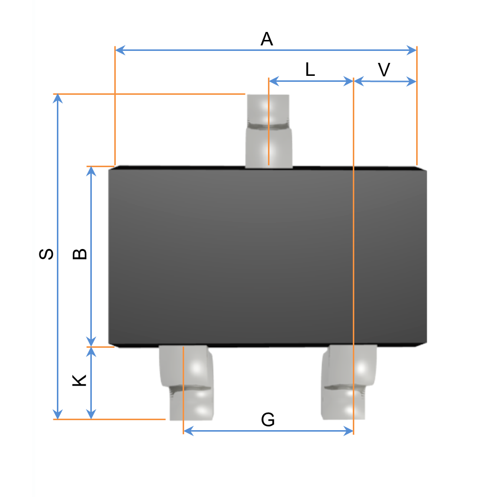
- SOT-23 – Small Outline Transistor: The SOR23 SMT / SMD Component Packages (Surface Mount Technology) is the most common outline for small signal transistors. The SOT23 has three terminals for a diode of transistor, but it can have more pins when it may be used for small integrated circuits such as an operational amplifier, etc. It measures 3 mm x 1.75 mm x 1.3 mm.
- SOT-223 – Small Outline Transistor: The SOT223 package is used for higher power devices. It is larger than the SOT-23 and it measures 6.7 mm x 3.7 mm x 1.8 mm. There are generally four terminals, one of which is a large heat-transfer pad. This enables heat to be transferred to the printed circuit board.
Integrated circuit SMD packages
There are many forms of package that are used for SMD ICs. Although there is a large variety, each one has the areas where its use is particularly applicable.
- SOIC – Small Outline Integrated Circuit : This SMD IC package has a dual in line configuration and gull wing leads with a pin spacing of 1.27 mm
- SOP – Small Outline Package: There are several versions of this SMD package:
- TSOP – Thin Small Outline Package: This SMD package is thinner than the SOIC and has a smaller pin spacing of 0.5 mm
- SSOP – Shrink Small Outline Package: This package has a pin spacing of 0.635 mm
- TSSOP – Thin Shrink Small Outline Package:
- QSOP – Quarter-size Small Outline Package: It has a pin spacing of 0.635 mm
- VSOP – Very Small Outline Package: This is smaller than the QSOP and has pin spacing of 0.4, 0.5, or 0.65 mm.
- QFP – Quad flat pack: The QFP is the generic type of flat package for ICs. There are several variants as detailed below.
- PLCC – Plastic Leaded Chip Carrier: This type of package is square and uses J-lead pins with a spacing of 1.27 mm.
- BGA – Ball Grid Array: The ball grid array SMD package has all its contact pads underneath the device package. Before soldering the pads appear as solder balls, giving rise to the name.
Placing the contacts underneath the device reduces the area required whilst maintaining the number of connections available. This format also overcomes some of the problems of the very thin leads required for the quad flat packs and makes the package physically more robust. The ball spacing on BGAs is typically 1.27 mm.

Although there appear to be very many different SMD packages, the fact that there are standards reduces the number and it is possible to set up printed circuit board design packages to accommodate them, along with proven pad sizes on the boards. In this way the packages enable high quality printed circuit board assembly and the reduction in overall number of variables within a design.