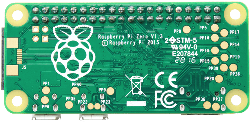
As you know I made some PDB’s in the past for some projects. From “Normal” components I switched over to SMD. But now I want to make things as small as possible. So I was thinking about a project I did a time ago, with a Raspberry Pi Zero W. This raspberry has so called ‘test pad’s’ I used Pogo pin’s to connect one PCB to another. This give me the idea to make my High Density Integration Connector or in short HDI Connector•.
Research
First I’m going to do some research. This means I gonna do a detailed study of a subject, especially in order to discover ‘new’ information or reach a ‘new’ understanding. So below I’m gonna show you which information I gathered and how I used it. Let’s start with the name HDI Connector •.

High Density Integration
A high density integration means a large number of components (usually transistors, in contexts where integration density is being discussed) in a small area. Because I’m gonna use a high amount of pogo pins on a small area. The HDI is therefore appropriate for my Connector. That’s why I called it HDI Connector •
Pin header
In the past I used a pin header as a connector to program my microcontroller (MCU for microcontroller unit). A pin header (or simply header) is a form of electrical connector. A male pin header consists of one or more rows of metal pins moulded into a plastic base, often 2.54 mm (0.1 in) apart, though available in many spacings. Male pin headers are cost-effective due to their simplicity. The female counterparts are sometimes known as a female socket header, though there are numerous naming variations of male and female connectors. Historically, headers are sometimes called “Berg connectors“,but headers are manufactured by many companies.
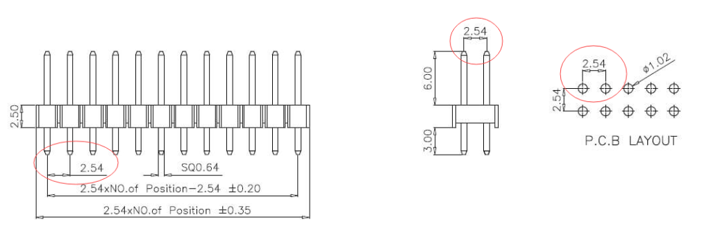
Normally pin headers are through-hole devices THD or THT (Through-hole technology), but surface-mount devices SMD or SMT (Surface-mount technology) exist too. In the SMD case, the solder side of the pins are bent on a 90 degree angle so as to be soldered to pads on the PCB. On single row SMD headers the pins are bent alternating to one side or the other, on dual row SMD headers the pins are simply bent outwards. If pin headers are optional, the THD variant is often chosen for ease of manual assembly. Headers can be either straight (vertical) or right-angle, the latter form is sometimes used to connect two PCBs together horizontally. Most often, headers are available in one or two rows, though three or more rows are available from some manufacturers. They are often sold as long strips (typically 36 / 40 / 50 pins) which can easily be cut apart to a required number of pins. Many pin lengths are available to minimise labor during PCB assembly. Male pin headers are often associated with ribbon cable connectors. When used alone, they can be recipients of jumpers, which have spacings of 2.54 mm (0.1 in) and 2.00 mm (0.079 in). Header types can be categorized by their pitch (uniform distance between pins measured from center to center). Some common header pitches are:
- 5.08 mm (0.200 in)
- 3.96 mm (0.156 in)
- 2.54 mm (0.100 in) with 0.64 mm (0.025 in) square pins or precision machined 0.50 mm (0.020 in) round pins
- 2.00 mm (0.079 in) with 0.50 mm (0.020 in) square pins
- 1.27 mm (0.050 in)
- 1.00 mm (0.0394 in)
This information is used in my designing phase later on.

Testing pads
For the first time I noticed these so called testing pads was on my Raspberry Pi Zero W in another project. I was looking for a alternative way to power this board, and the I found out about these pads. A test pad is a location within an electronic circuit that is used to either monitor the state of the circuitry or to inject test signals. Modern miniature surface-mount electronics often simply have a row of unlabelled, tinned solder pads. The device is placed into a test fixture that holds the device securely, and a special surface-contact connector plate is pressed down onto the solder pads to connect them all as a group.
Pogo-pin
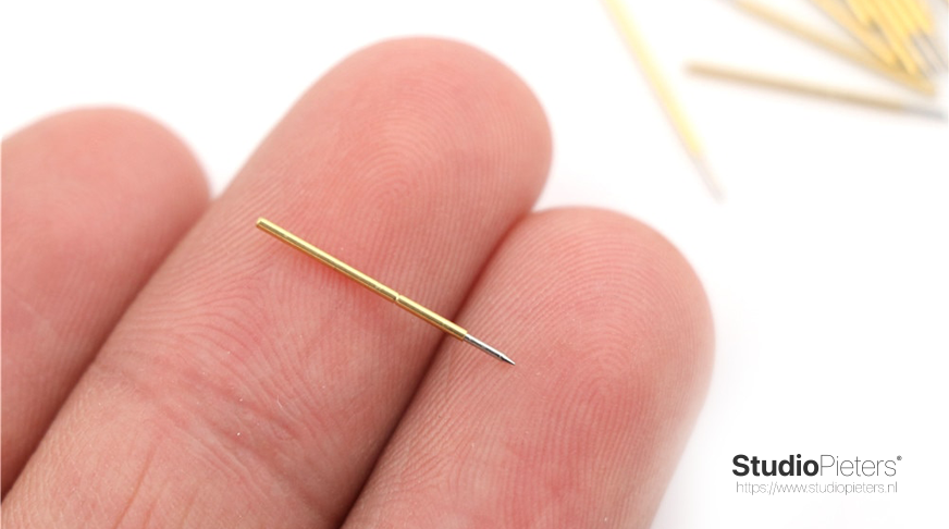
The pogo pin I also used before in my Raspberry Pi Zero W project. A pogo pin or spring-loaded pin is a type of electrical connector mechanism that is used in many modern electronic applications and in the electronics testing industry. They are used for their improved durability over other electrical contacts, and the resilience of their electrical connection to mechanical shock and vibration.
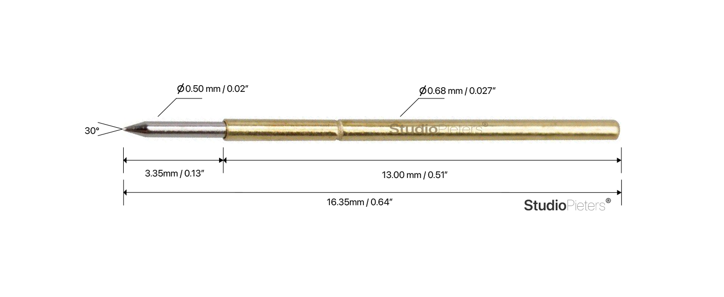
The name pogo pin comes from the pin’s resemblance to a pogo stick – the integrated helical spring in the pin applies a constant normal force against the back of the mating receptacle or contact plate, counteracting any unwanted movement which might otherwise cause an intermittent connection. This helical spring makes pogo pins unique, since most other types of pin mechanisms use a cantilever spring or expansion sleeve. A complete connection path requires a mating receptacle for the pin to engage, which is termed a target or land. A pogo target consists of a flat or concave metal surface, which unlike the pins, has no moving parts. Targets may be separate components in the complete connector assembly, or in the case of printed circuit boards, simply a plated area of the board. Spring-loaded pins are precision parts fabricated with a turning and spinning process which does not require a mould, thus allowing the production of smaller quantities at a lower cost.
The idea
So now that I have gathered al knowledge I need I can start making my idea of a HDI Connector•. The upload procedure for ESP8266 boards is a little different from a standard Arduino procedure. Most Arduino’s will automatically reset when a new program is being uploaded, and will automatically enter programming mode. On some ESP boards you have to manually enter programming mode, and on the bare-bones modules, you even have to reset them manually. However, there are some simple circuits you can use to get automatic uploads. you can read more about this in my blog here.
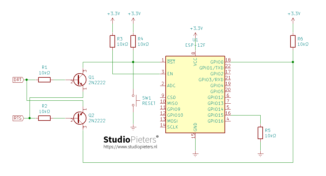
Now that I have a scheme to automatically Program and Reset my ESP. I need a efficient way for a connector with a smaal footprint. This way I can eliminate two big buttons for one micro button (Reset) and the elimination of a big header on my PCB to program my ESP module.
3D Design
For my designing part I used AutoCAD Fusion 360. Autodesk offers a full version of Fusion 360 for free to students and educators. Hobbyists can use a feature-limited Fusion 360 provided it’s for noncommercial reasons, and small startups can access download, and use the full Fusion 360 software for free. Preceding all of these though is the fully functional Fusion 360 free trial, which lets you test the software out before locking yourself into one of the various license types.
First of all, anyone interested in getting acquainted with this software can utilize a 30-day Fusion 360 free trial version from Autodesk’s website. Here’s how you do it:
- Visit Autodesk’s Fusion 360 website.
- Click DOWNLOAD FREE TRIAL
- Fill in your information. Click DOWNLOAD FREE TRIAL.
- The website automatically detects your operating system and starts the download of the appropriate installer.
- Install the free Fusion 360 trial.
This trial version includes all of the features of the full version. So, if you are looking to test a particular application of Fusion 360, or want to see how it operates for a particular workflow, this may be the optimal choice to test things out. Of course, you are limited to 30 days, so don’t get too reliant on it unless you plan on switching to another version.
The personal license grants access to most of the features of the full version, but has several limits. You will not be able to import and export as wide a variety of file types, and some of the workflows will be limited. Additionally, you will not have access to the cloud features. The license is renewed on a yearly basis. This license is for those of us who wish to use Fusion around the workshop and in our various hobbies. While you won’t have quite as many high-end features and rendering options, designing for 3D printing and basic CNC work will still function just fine. If you use professional CAD at work, this may be the perfect option for you to apply some of your skills to hobbies around the house and in your garage.
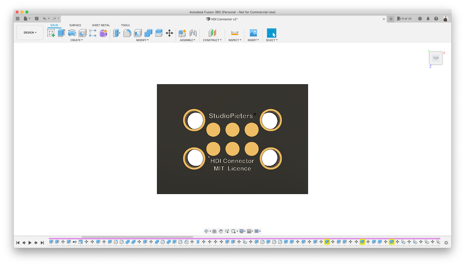
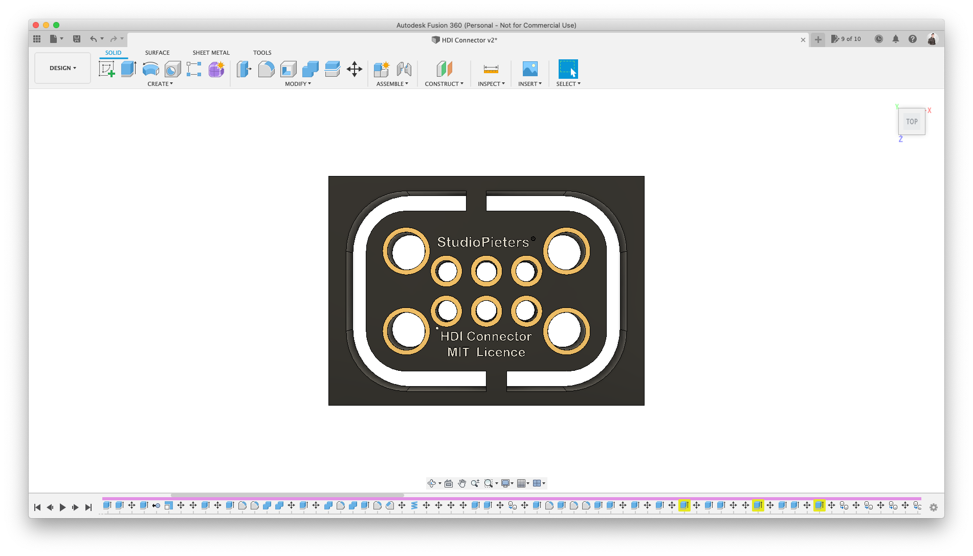
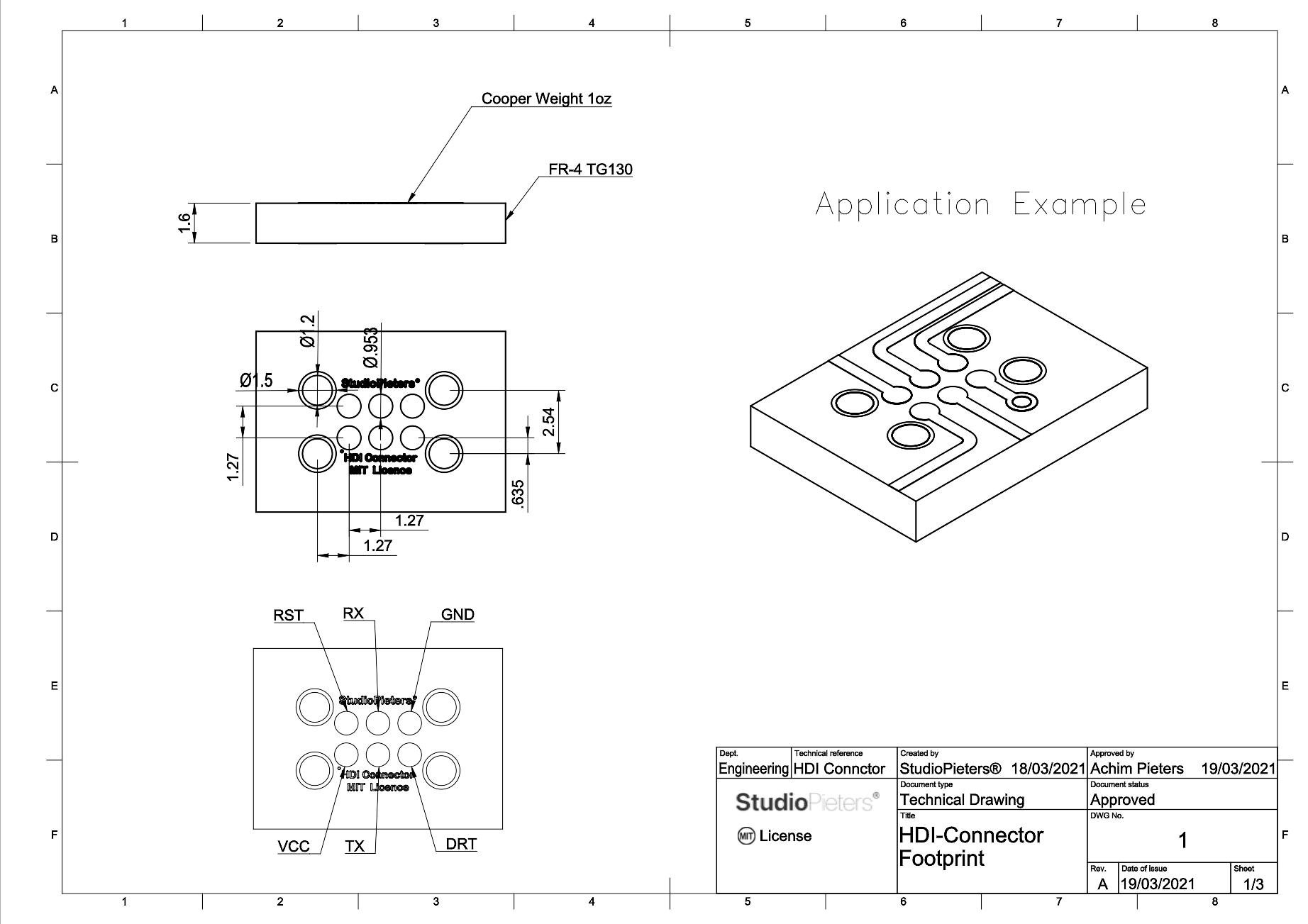
HDI Connector • Footprint
The first ting I did is designing a footprint as small as possible. Here for I used common header pitch dimensions as you can see in my AutoCAD Fusion 360 Drawing below.
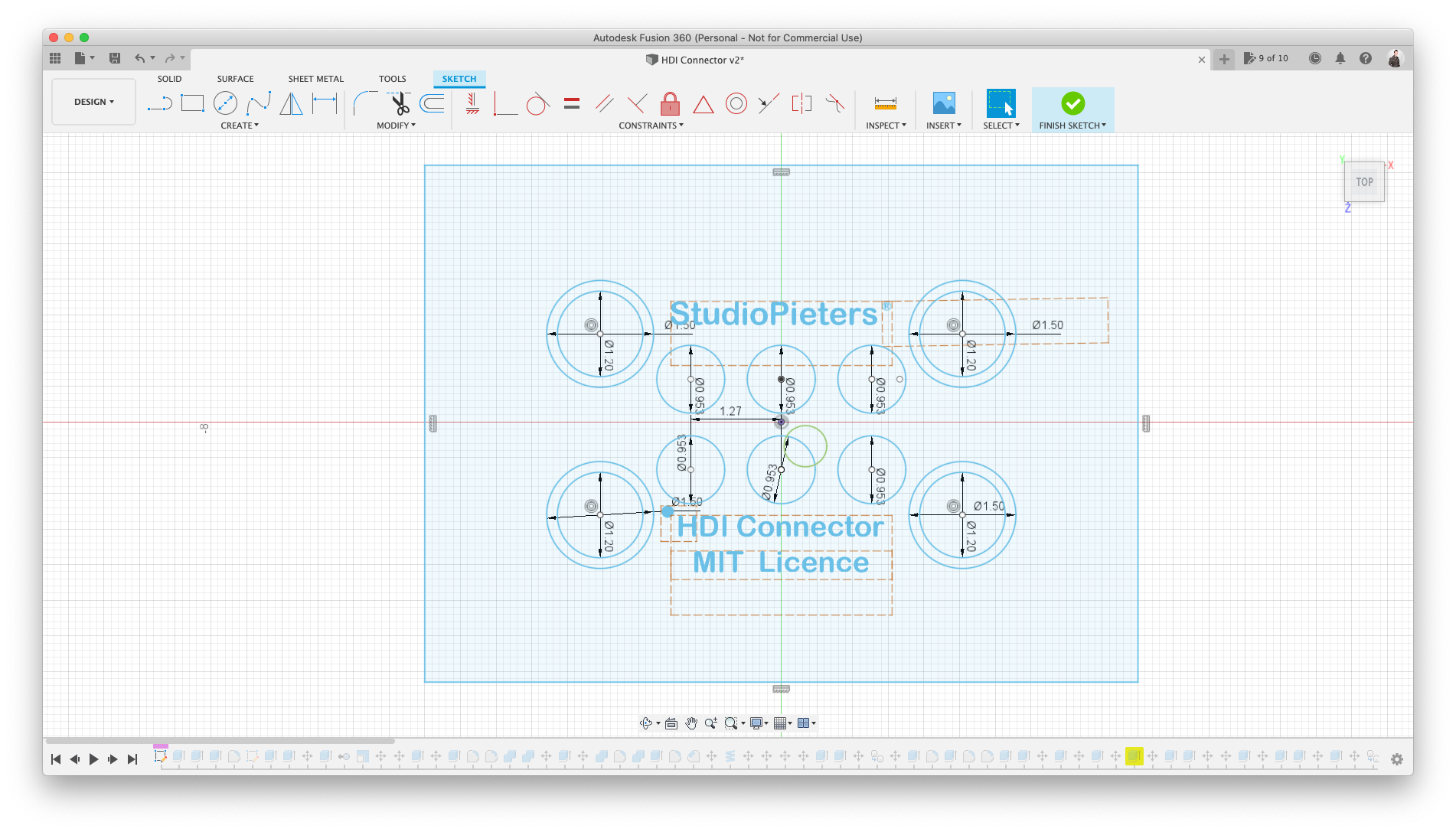

After some thinking about the minimal sizes and a way to keep te connector in place, I made it into a 3D model.
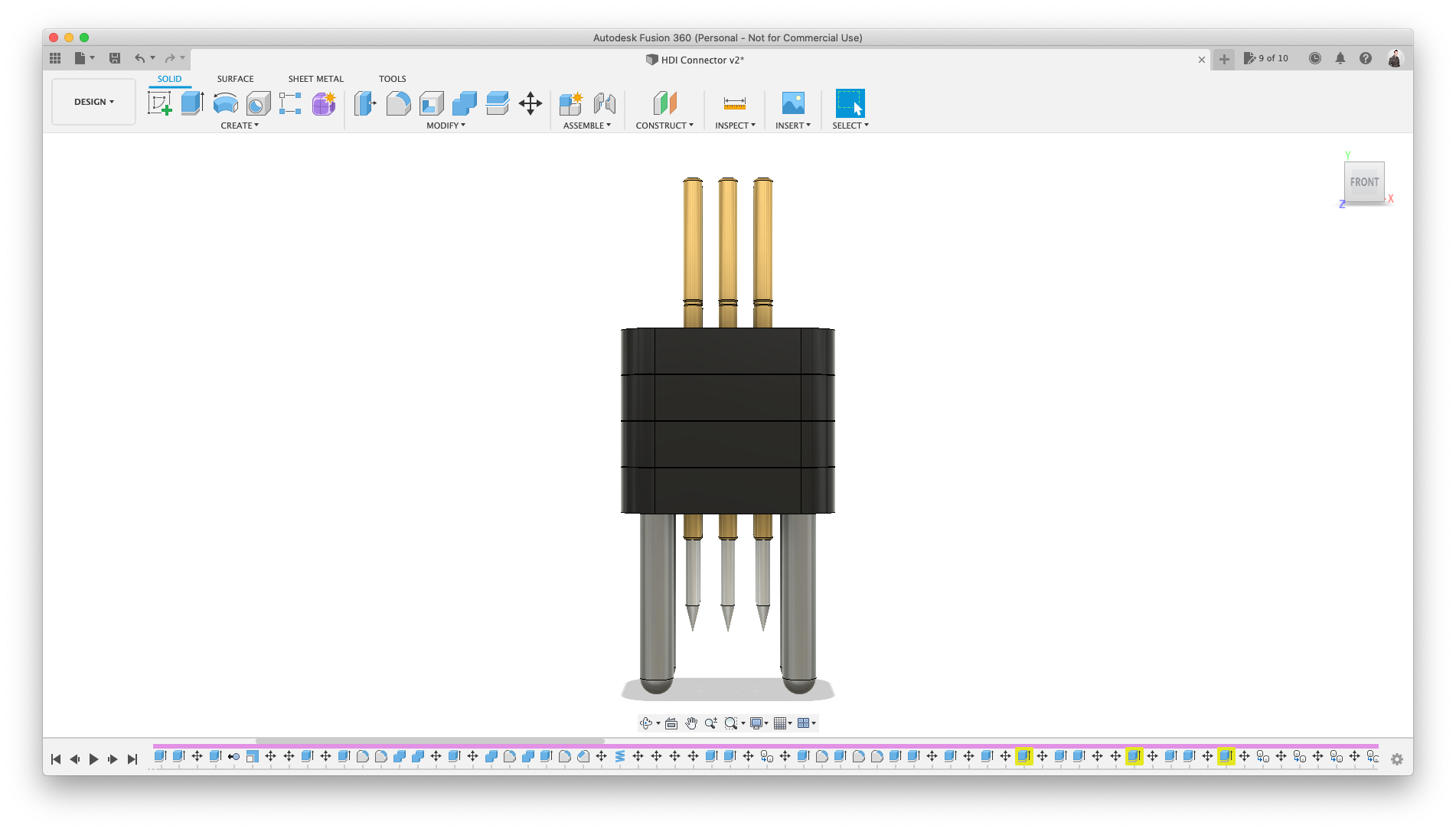
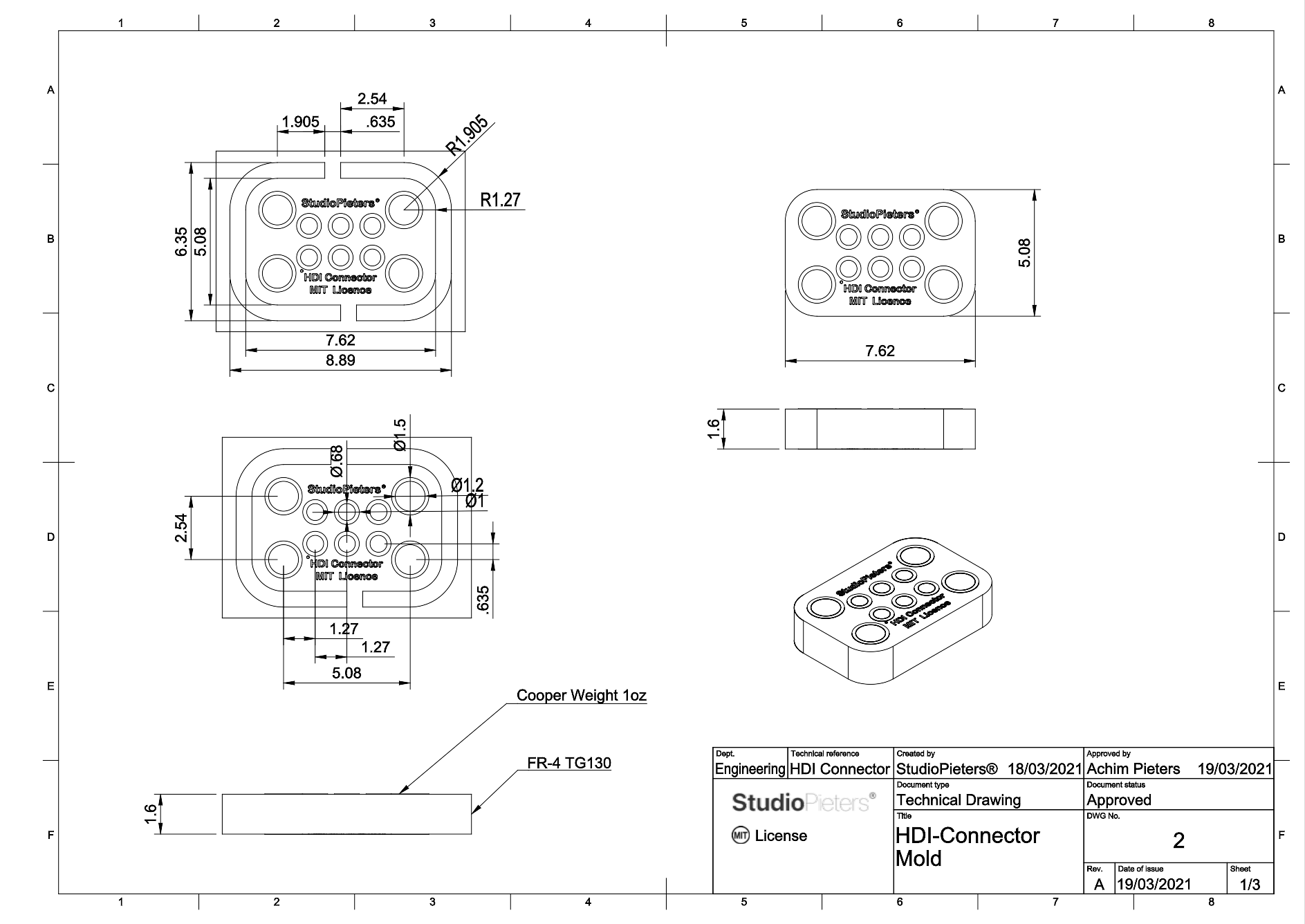
HDI Connector • Mould
Now that I know how the Footprint is going to look like I can make the mould for the matching connector. The Idea is to use (excess) PCB material to make the mould for a connector, this way ‘everybody‘ can make this connector, because all dimensions, drilling etc. Is already done. the only thing is the assembly of such one.
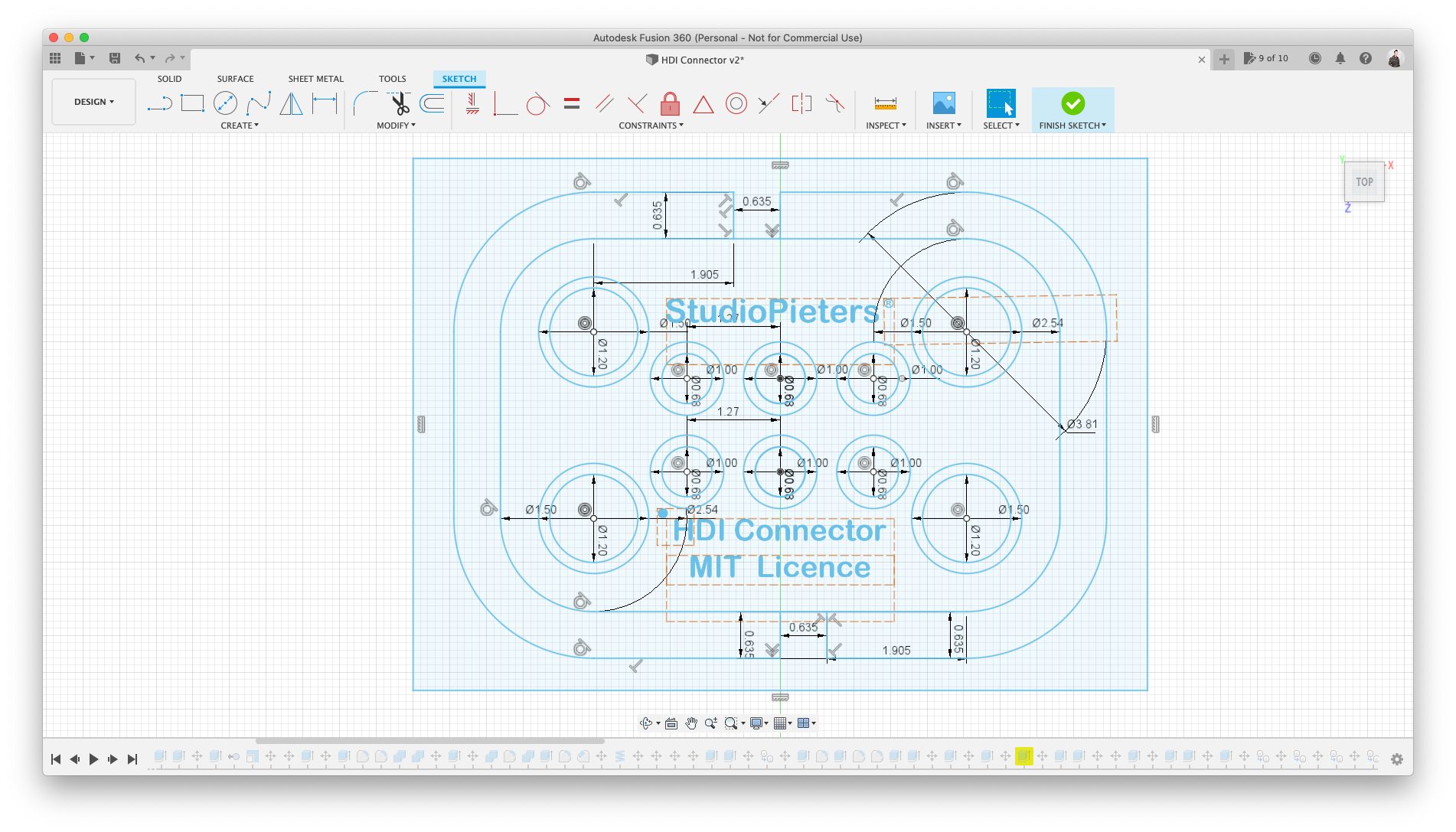
After Designing, rethinking and adjusting I made the 3D model, as shown below.
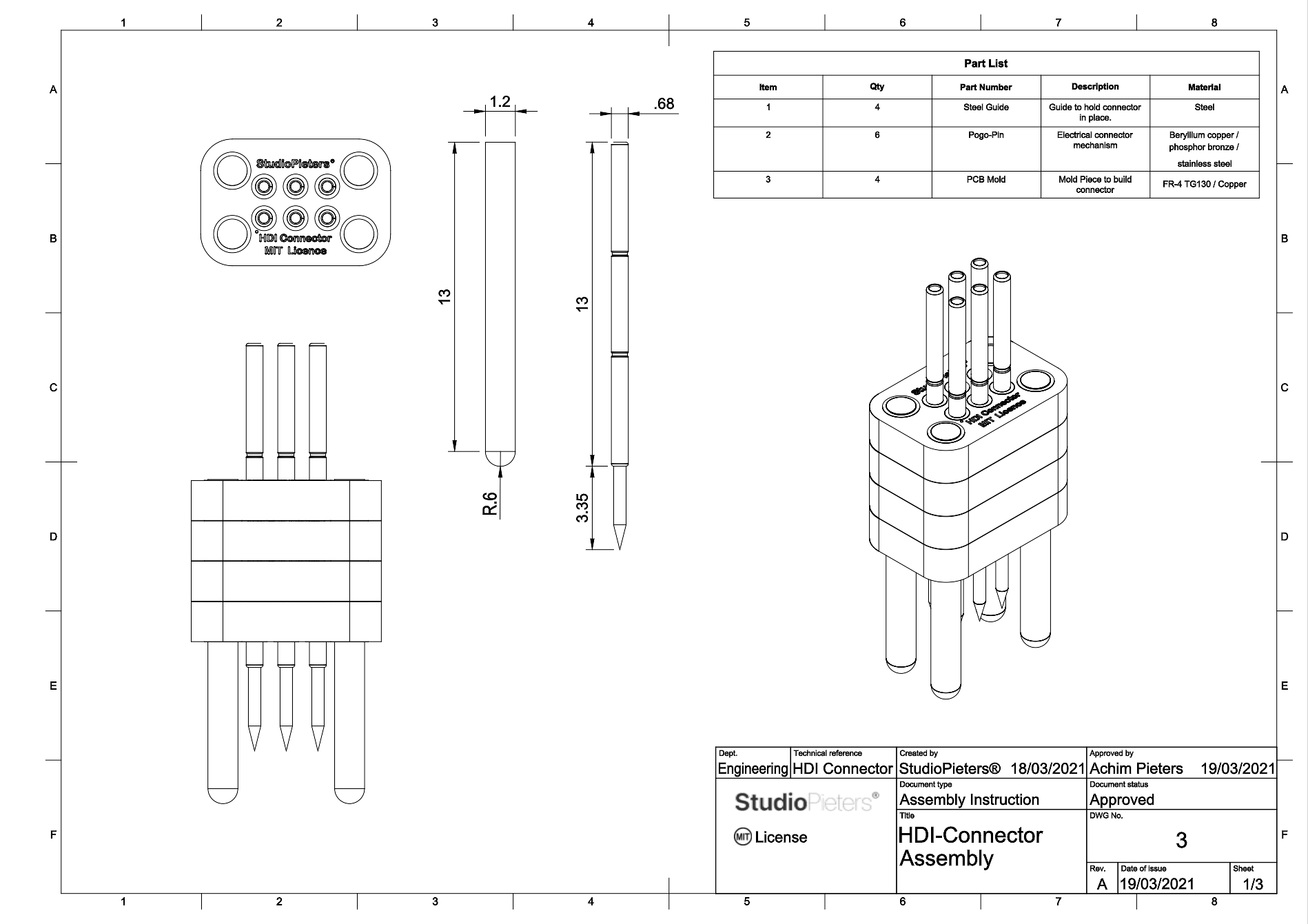
HDI Connector • Assembly
For the assembly of the HDI Connector• you need four pieces of the mould part, Six Pogo pin’s and 4 Steel rod’s with a dimensions of 1.2 mm diameter and a with a length of 13 mm.
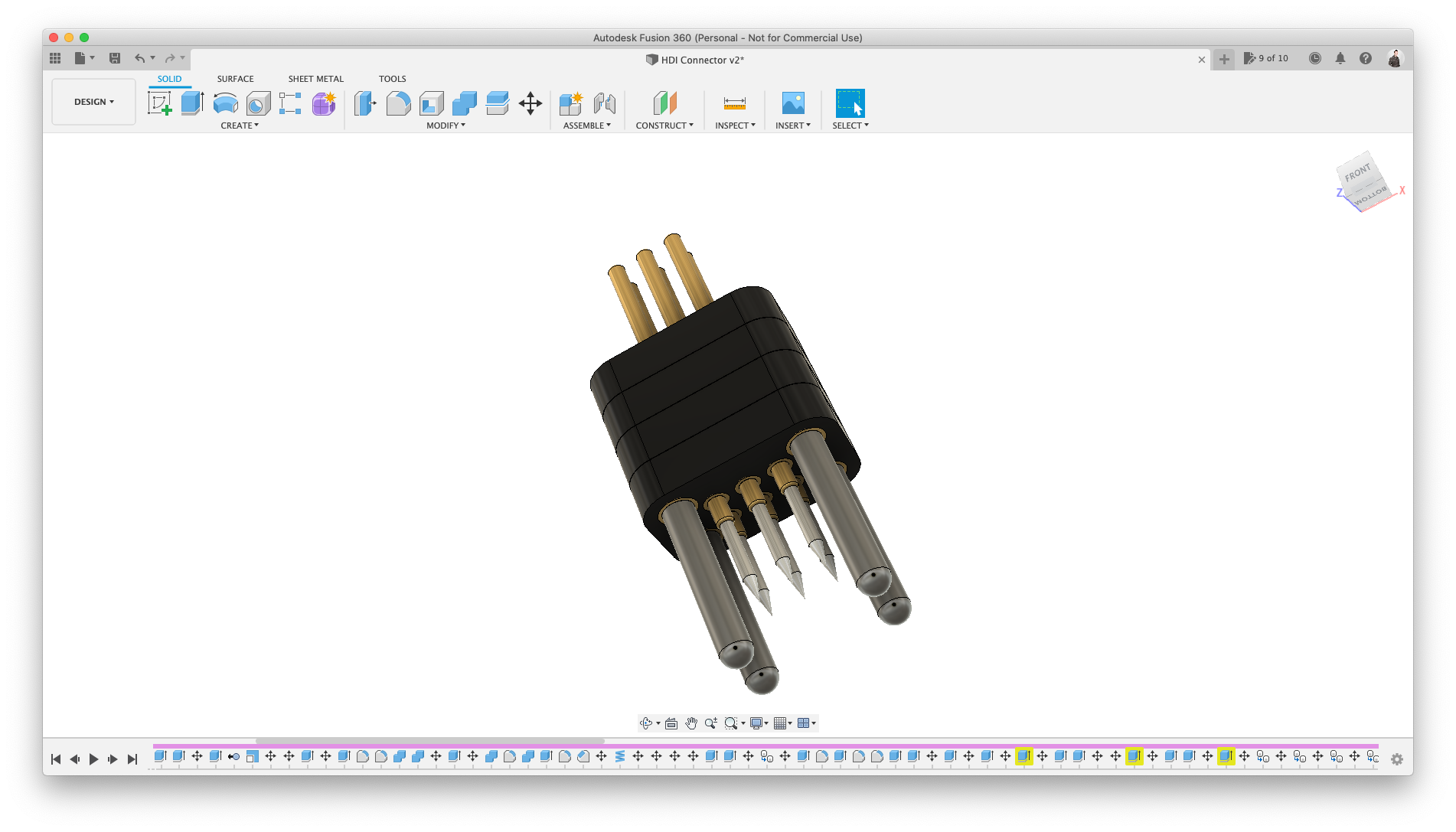
Place the steel guides in the outer four holes. You can solder them to keep them in place. Here after you can place the pogo pins. make sure the ‘copper’ tube sticks out 1mm on the bottom. This 1 mm is without the silver needle.
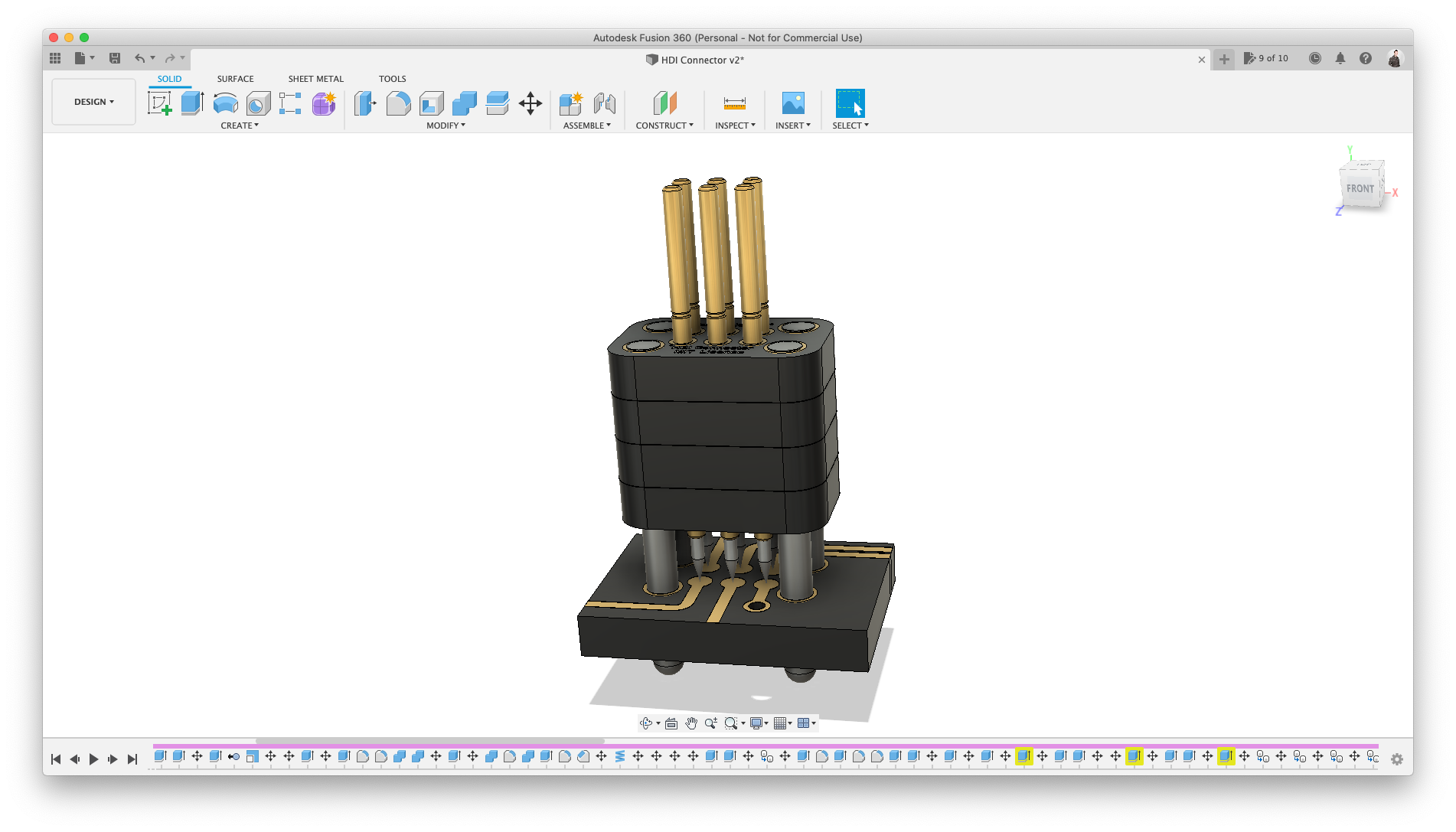
HDI Connector • Application example
In the image blow you see How it will look when the assembled connector is placed on the footprint. To keep the connector in place, bend the steel guides very slightly to the out side this way they will get “stuck” in the holes of the footprint.

KiCad
For all my PCB design I use KiCAD. KiCad (pronounced “Key-CAD”) is a free software suite for electronic design automation (EDA). It facilitates the design of schematics for electronic circuits and their conversion to PCB designs. KiCad was originally developed by Jean-Pierre Charras. It features an integrated environment for schematic capture and PCB layout design. Tools exist within the package to create a bill of materials, artwork, Gerber files, and 3D views of the PCB and its components.
KiCad was created in 1992 by Jean-Pierre Charras while working at IUT de Grenoble. Since then KiCad has gained a number of both volunteer and paid contributors. Notably in 2013 the CERN BE-CO-HT section started contributing resources towards KiCad to help foster open hardware development by helping improve KiCad to be on par with commercial EDA tools.
KiCad adopted a point release versioning scheme in December 2015 starting with KiCad 4.0.0. This was the first release featuring the more advanced tools implemented by CERN developers. CERN hopes to contribute further to the development of KiCad by hiring a developer through donations. Contributions may be made through the links on KiCad’s website.
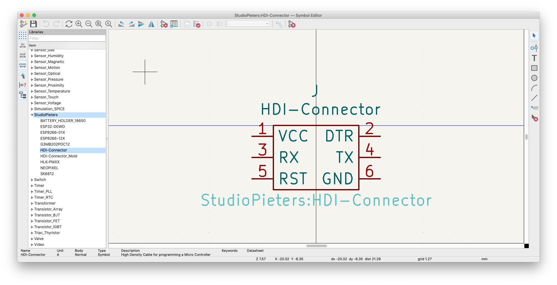
HDI Connector • Footprint Symbol
Before I can use my newly designed HDI Connector • I need to make a symbol in KiCAD, First I make the Footprint symbol. This can be a very simple design. I only have to define which pins is which, eg Pin1 is VCC, Pin 2 is DTR, etc.
HDI Connector • Footprint
Designing the footprint was a little more challenging, The dimensions have to right just as defined in my Fusion 360 drawing. If the Dimensions do not match things will not align and eventually not work.
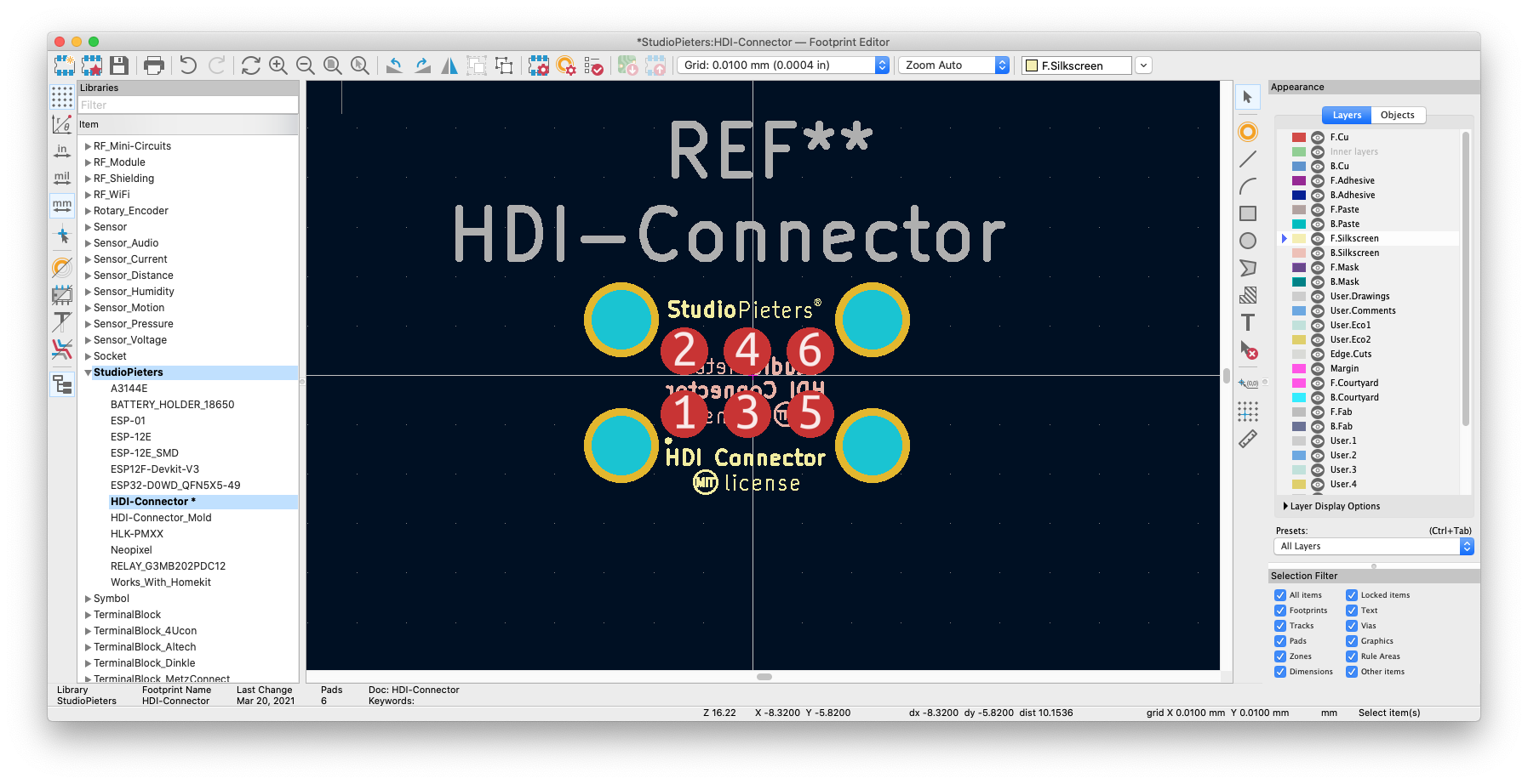
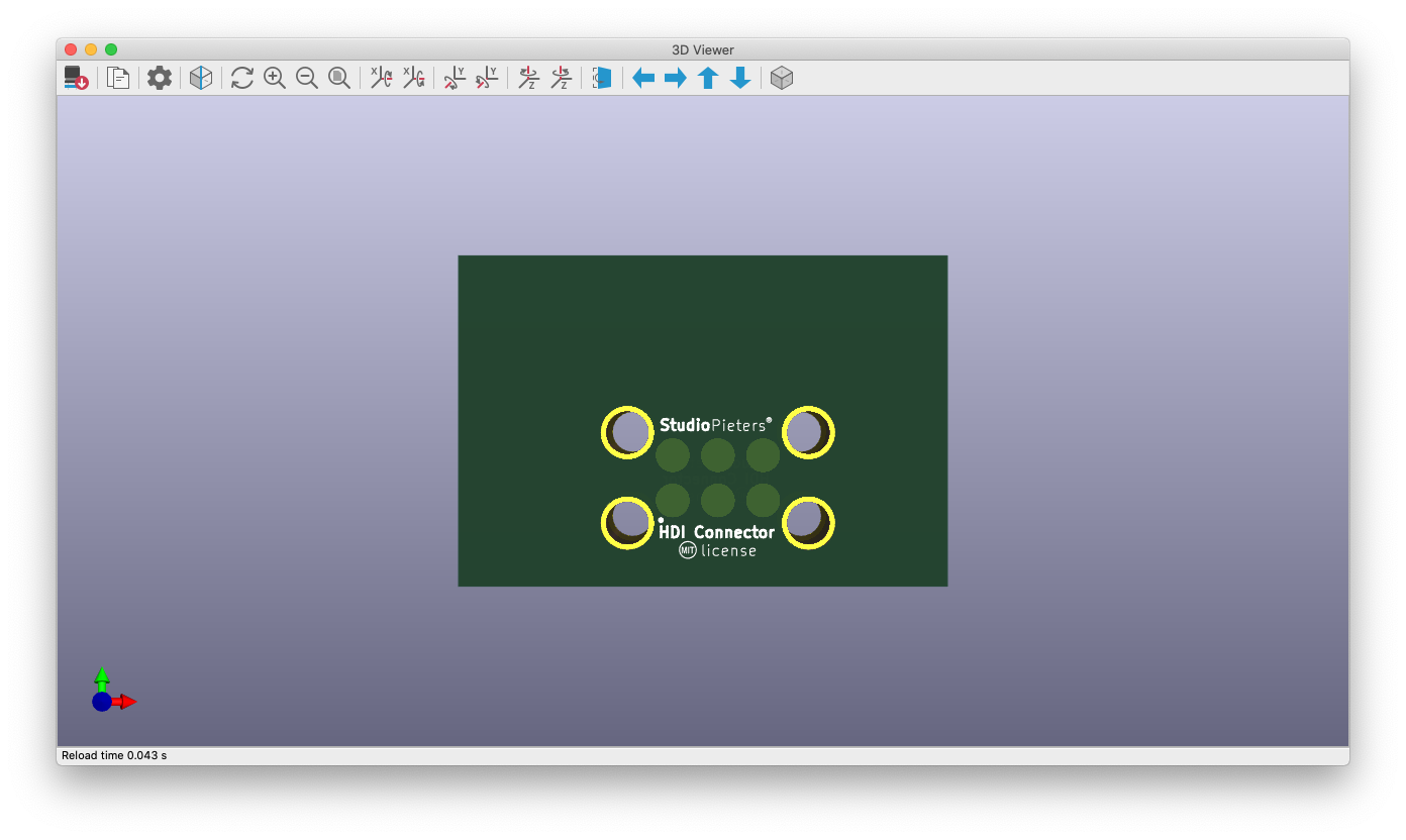
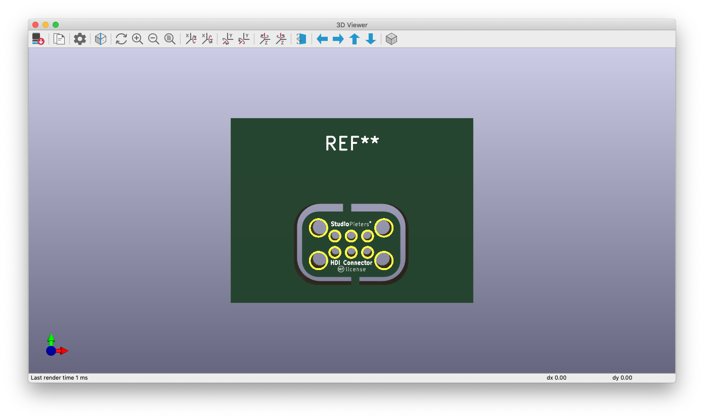
Kicad has a nice feature build into its interface a 3D viewer. This way you can see how your design will look on you PCB Later on.

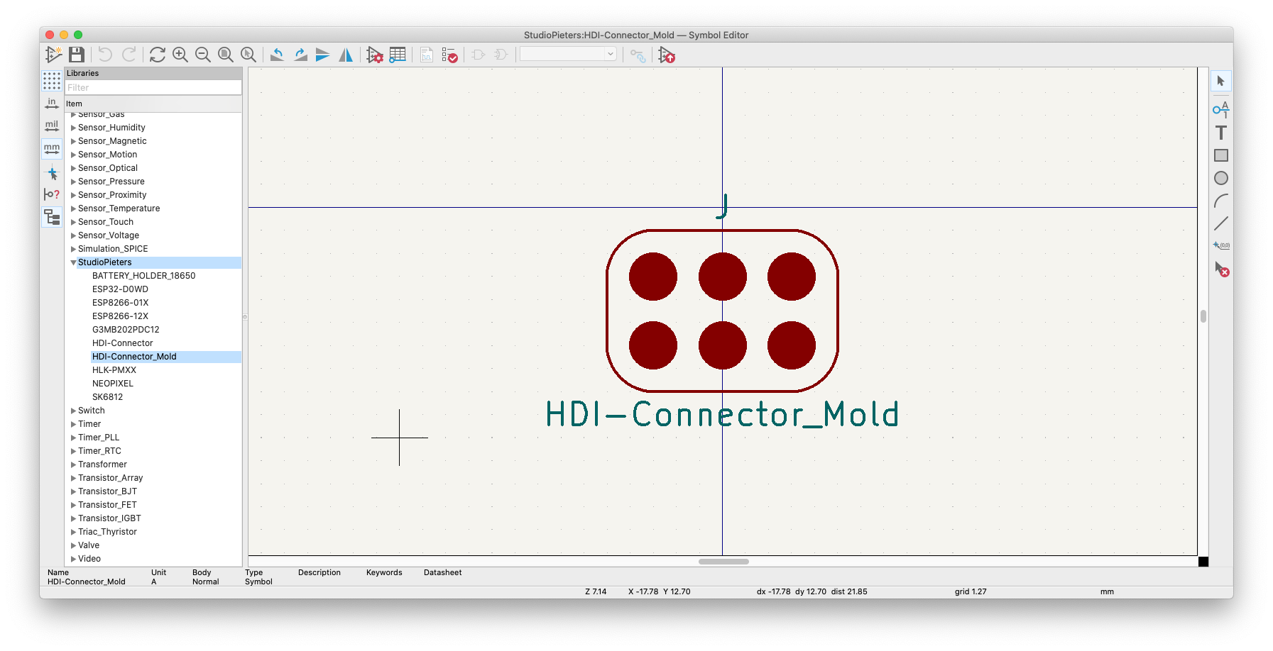
HDI Connector • Symbol Mould
Now that the footprint is finishes its time to make the symbol for the Mould in Kicad. The mould Symbol does not need any connections, as it only is a Mould and noting more.
HDI Connector • Mould
Also Designing the Mould footprint is a challenging task. Also here the correct dimensions ar of the most essence.
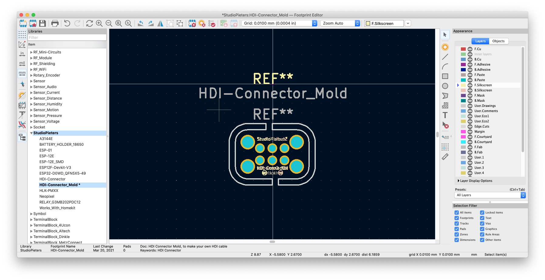
After some time I finished the footprint. I reviewed it in KiCAD’s 3D viewer.
HDI Connector • Application example
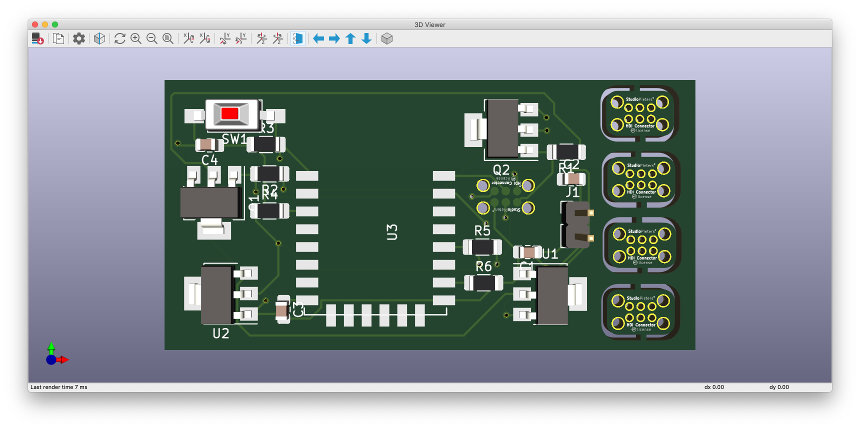
Now that all parts are made, its time to see if it works. I make a “standard” scheme with a ESP Module with Auto Program & Reset function and of course my HDI Connector• Footprint and mould.
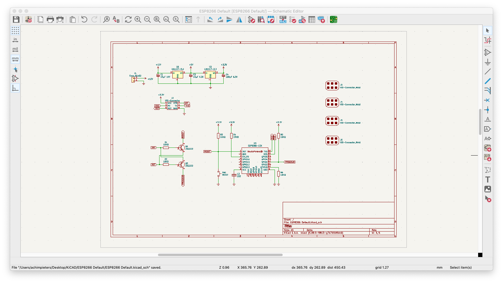
After the scheme is finalised I only need to place all parts and connect all parts wit a Line. I didn’t really looked to make a small as possible PCB, nor I looked it the Components are place the most efficient way. I Aly want to see how my newly made parts look in a “real life” environment .
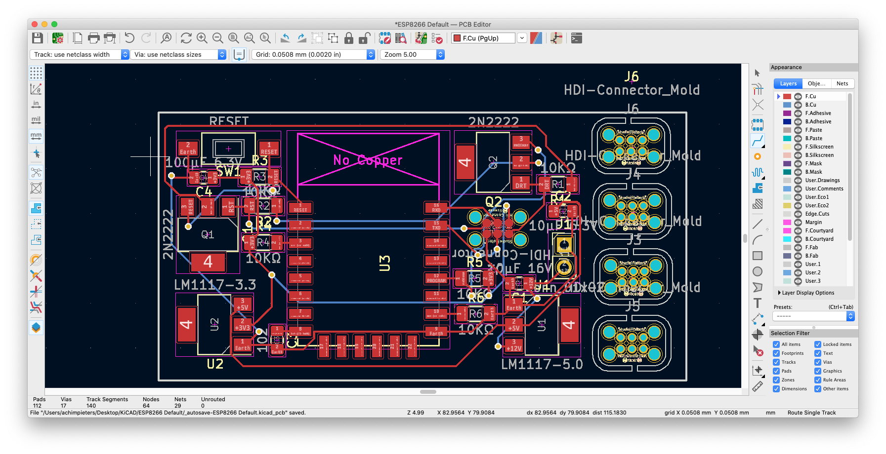
After This is done, I opened KiCAD’s 3D viewer again, and this looks good!
Technical Drawings
Despite I already made the KiCAD parts, free to download below. I made some technical drawings. I made this whole project under MIT licence so is free to use for everyone, as long as you obey the Licence terms.

The technical drawing of the HDI Connector • Footprint design.
The technical drawing of the HDI Connector • mould design.
The technical drawing of the HDI Connector • assembly design.
Download Files
You can download all files here. The download contains the Technical drawings, Autodesk Fusion360 files and Kicad Footprints.

License
Applications
Hardware, Documents & Files, Software
Benefits
Open license. Provides basic liability protections. Requires that the associated copyright notice is included in derived works. Roughly equivalent to the the Simplified BSD License. Similar to the Modified BSD License, except does not prohibit the use of the name of the copyright holder in promotion.
License
Copyright (c) 2021 StudioPieters®
Permission is hereby granted, free of charge, to any person obtaining a copy of this hardware, software, and associated documentation files (the “Product”), to deal in the Product without restriction, including without limitation the rights to use, copy, modify, merge, publish, distribute, sublicense, and/or sell copies of the Product, and to permit persons to whom the Product is furnished to do so, subject to the following conditions:
The above copyright notice and this permission notice shall be included in all copies or substantial portions of the Product.
THE PRODUCT IS PROVIDED “AS IS”, WITHOUT WARRANTY OF ANY KIND, EXPRESS OR IMPLIED, INCLUDING BUT NOT LIMITED TO THE WARRANTIES OF MERCHANTABILITY, FITNESS FOR A PARTICULAR PURPOSE AND NONINFRINGEMENT. IN NO EVENT SHALL THE AUTHORS OR COPYRIGHT HOLDERS BE LIABLE FOR ANY CLAIM, DAMAGES OR OTHER LIABILITY, WHETHER IN AN ACTION OF CONTRACT, TORT OR OTHERWISE, ARISING FROM, OUT OF OR IN CONNECTION WITH THE PRODUCT OR THE USE OR OTHER DEALINGS IN THE PRODUCT.

DO YOU HAVE ANY QUESTIONS? LEAVE A COMMENT DOWN HERE.