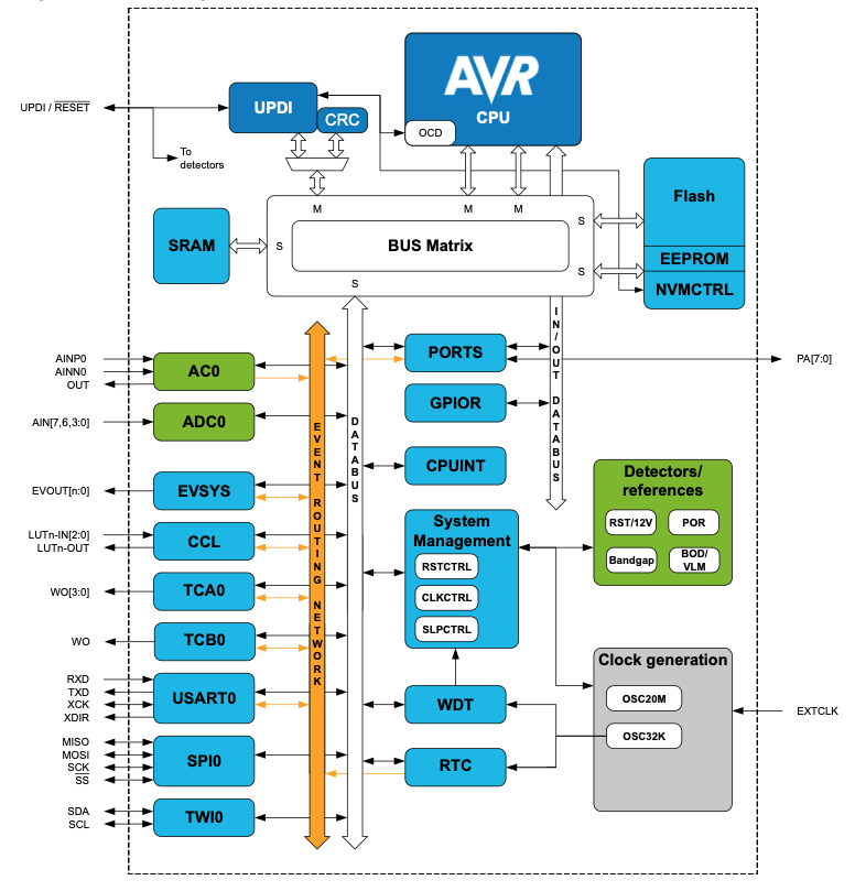
The ATtiny214/414/814 microcontrollers are using the high-performance low-power AVR® RISC architecture, and is capable of running at up to 20MHz, with up to 2/4/8KB Flash, 128/256/512bytes of SRAM and 64/128bytes of EEPROM in a 14- pin package. The series uses the latest technologies with a flexible and low power architecture including Event System and SleepWalking, accurate analog features and advanced peripherals. Capacitive touch interfaces with driven shield are supported with the integrated QTouch® peripheral touch controller.
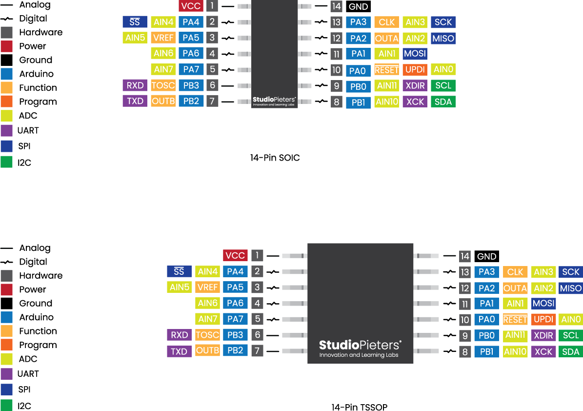
ATTiny414 – Pinout – Peripherals
The ATTiny414 peripherals include:
- FLASH (RAM) 4K (256/*512)
- 12 x Programmable I/O lines
- 12 x Channel 10-bit ADC with Voltage Reference
- 1 x UPDI
- 1 x SPI
- 1 x UART
- 1 x I2C
The ADC (analogue to digital converter) and DAC (digital to analogue converter) features are assigned to specific static pins. For in-depth information, I refer you to the datasheet here: DATASHEET

Additionally, there are pins with specific features that make them suitable or not for a particular project. The following table shows what pins are best to use as inputs, outputs and which ones you need to be cautious.
The pins highlighted in Green are OK to use. The ones highlighted in Orange are OK to use, but you need to pay attention because they may have an unexpected behaviour, mainly at boot. The pins highlighted in Red are not recommended to use as inputs or outputs.
| PIN Nr. | Input | Output | Notes |
| 1 | – | – | VCC |
| 2 | OK | OK | PA4, AIN4, SS |
| 3 | OK | OK | PA5, VREF, AIN5 |
| 4 | OK | OK | PA6, AIN6 |
| 5 | OK | OK | PA7, AIN7 |
| 6 | OK | OK | PB3, TOSC, RXD |
| 7 | OK | OK | PB2, OUTB, TXD |
| 8 | OK | OK | PB1, AIN10, XCK, SDA |
| 9 | OK | OK | PB0, AIN11, XDIR, SCL |
| 10 | OK | OK | PA0, RESET, UPDI, AIN0 |
| 11 | OK | OK | PA1, AIN1, MOSI |
| 12 | OK | OK | PA2, OUTA, AIN2, MISO |
| 13 | OK | OK | PA3, CLK, AIN3, SCK |
| 14 | – | – | GND |

Analog to Digital Converter (ADC)
The Analog-to-Digital Converter (ADC) peripheral features a 10-bit Successive Approximation ADC (SAR), with a sampling rate up to 115 ksps at 10-bit resolution (150 ksps at 8-bit). The ADC is connected to a 6-channel analogue multiplexer, which allows twelve single-ended voltage inputs. The single-ended voltage inputs refer to 0V (GND). The ADC input channel can either be internal (e.g. a voltage reference) or external through the analogue input pins.

I2C
The Two-Wire Interface (TWI) is a bidirectional, two-wire communication interface (bus) with a Serial Data Line (SDA) and a Serial Clock Line (SCL). The TWI bus connects one or several client devices to one or several host devices. Any device connected to the bus can act as a host, a client, or both. The host generates the SCL by using a Baud Rate Generator (BRG) and initiates data transactions by addressing one client and telling whether it wants to transmit or receive data. The BRG
is capable of generating the Standard mode (Sm) and Fast mode (Fm, Fm+) bus frequencies from 100 kHz up to 1 MHz. The TWI will detect Start and Stop conditions, bus collisions, and bus errors. Arbitration lost, errors, collision, and clock hold are also detected and indicated in separate status flags available in both Host and Client modes. The TWI supports multi-host bus operation and arbitration. An arbitration scheme handles the case where more than one host tries to transmit data at the same time. The TWI also supports Smart mode, which can auto-trigger operations and thus reduce software complexity. The TWI supports Quick Command mode where the host can address a client without exchanging data.
- PA1 (SDA)
- PA2 (SCL)
SPI
The Serial Peripheral Interface (SPI) is a high-speed synchronous data transfer interface using three or four pins. It allows full-duplex communication between an AVR® device and peripheral devices, or between several microcontrollers. The SPI peripheral can be configured as either host or client. The host initiates and controls all data transactions. The interconnection between host and client devices with SPI is shown in the block diagram. The system consists of two shift registers and a server clock generator. The SPI host initiates the communication cycle by pulling the desired client’s Client Select (SS) signal low. The host and client prepare the data to be sent to their respective shift registers, and the host generates the required clock pulses on the SCK line to exchange data. Data are always shifted from
host to client on the host output, client input (MOSI) line, and from client to host on the host input, client output (MISO) line.
- PA0 (CS)
- PA1 (MOSI)
- PA3 (SCK)
- PA2 (MISO)
UPDI – Unified Program and Debug Interface
The Unified Program and Debug Interface (UPDI) is a proprietary interface for external programming and on-chip debugging of a device.
The UPDI supports programming of non-volatile memory (NVM) space; FLASH, EEPROM, fuses, lock bits, and the user row. In addition, the UPDI can access the entire I/O and data space of the device. Programming and debugging are done through the UPDI Physical interface (UPDI PHY), which is a 1- wire UART-based half duplex interface using the RESET pin for data reception and transmission.
More information about the UPDI programmer can be found here: https://www.studiopieters.nl/updi
Pin current drawn
The absolute maximum current drawn per pin is 40mA according to the “Absolute Maximum Ratings” section in the ATTiny414 datasheet.

Overview
The ATTiny 0/1/2 series Microcontroller is one of the most versatile chips on the market today, and that’s why we decided to focus on it in this blog. This blog displays most of its capabilities, but there are also more advanced options, which we did not go into in this post. Please see the technical document of your chip’s manufacturer for more information. For in-depth information, I refer you to the datasheet here: DATASHEET
The important thing to know when you choose a board for your project is its capabilities and limitations. It’s also essential to understand the different communication protocols that the board uses. Of course, you don’t need to remember all of this information, you can always go back to this post and read the relevant information for you (this is a good time to bookmark this Blog btw).