
Electronics
KiCad 6 Track Width Template
A KiCad 6 template with 24 predefined track widths from 4 to 50 mil, and how to import them into your own board.
- KiCad
- 2 min read

A KiCad 6 template with a ready-made list of track widths. Instead of typing each width into the board setup yourself, you import the list once, and then step through the sizes while you route.
It is for KiCad 6.0.10 and up.
What predefined sizes are for
The predefined sizes let you decide which track and via dimensions are available while you route. Net classes set the default dimensions for tracks and vias in different nets, but a list of sizes lets you step through them as you work. You may want a default track width of 0.2 mm on a board, with 0.3 mm for sections that carry more current, and 0.15 mm where space is tight. You define each of these in the board setup dialog, and then switch between them while routing.
What the template contains
The template defines 24 track widths, from 0.1016 mm (4 mil) up to 1.27 mm (50 mil), in steps of 0.0508 mm (2 mil):
| Width in mil | Width in mm |
|---|---|
| 4 | 0.1016 |
| 6 | 0.1524 |
| 8 | 0.2032 |
| 10 | 0.2540 |
| 12 | 0.3048 |
| 16 | 0.4064 |
| 20 | 0.5080 |
| 30 | 0.7620 |
| 40 | 1.0160 |
| 50 | 1.2700 |
The table shows a selection. The full list runs through every even number of mil from 4 to 50. The list of via sizes is left empty.
The project also holds default settings. The default net class has a track width of 0.25 mm, a via diameter of 0.8 mm with a 0.4 mm drill, and a clearance of 0.2 mm. The minimum track width is 0.2 mm, the minimum via diameter is 0.4 mm, the minimum annular width is 0.05 mm and the minimum through hole is 0.3 mm.
For track widths and the current they carry, the SMD reference sheets have a track width table.
How to use it
- Clone the repository:
git clone --recursive https://github.com/AchimPieters/KiCAD6-Trackwidth.git - Open KiCad 6.0.10 or newer and start your new design.
- When you are ready to design the PCB, open the KiCad PCB editor.
- Open the track width pull-down menu and choose Edit Pre-defined Sizes. The Board Setup window opens.
- In the left corner, click Import Settings from Another Board.
- Select this repository, the file
Track/Track.kicad_pcb, and click Import Settings.
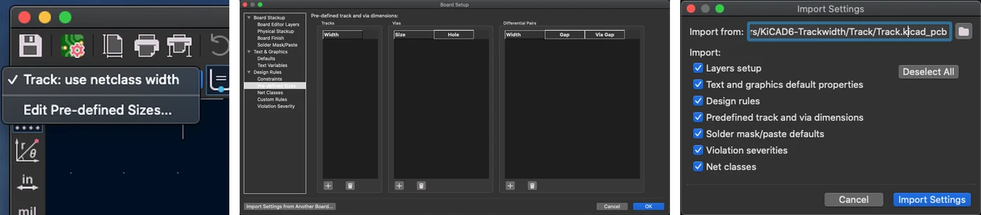
The import dialog lists what is copied: the layers setup, the text and graphics defaults, the design rules, the predefined track and via dimensions, the solder mask and paste defaults, the violation severities and the net classes. All are ticked by default, so untick what you do not want to replace in your own board.
A custom folder icon
The repository also has a folder icon, to find the right folder quickly. On a Mac, choose File, then Get Info, click the small folder icon at the top of the info window, and drag the new icon onto it.
Good to know
- The template is under the MIT licence.
- The first release, 0.0.1, was made on 26 August 2022.
Everything is in the KiCAD6-Trackwidth repository on GitHub.
Related
 3D printing
3D Printed Case for a Homebridge Raspberry Pi
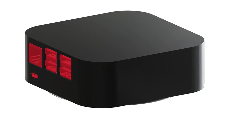
A black 3D printable case with openings for the network port, USB ports and power connector, for a Raspberry Pi that runs Homebridge.
Read more
3D printing
3D Printed Case for a Homebridge Raspberry Pi
A black 3D printable case with openings for the network port, USB ports and power connector, for a Raspberry Pi that runs Homebridge.
Read more
 Electronics
Switch a Relay or a Led from Homebridge with an ESP-01
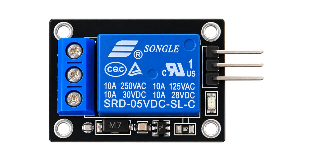
An ESP-01 web server that sets GPIO2 high or low, the basic building block for switching lights and relays from Homebridge.
Read more
Electronics
Switch a Relay or a Led from Homebridge with an ESP-01
An ESP-01 web server that sets GPIO2 high or low, the basic building block for switching lights and relays from Homebridge.
Read more
 Software
ESP32 SHT3x Driver for ESP-IDF
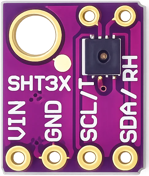
A driver for Sensirion SHT3x temperature and humidity sensors on the ESP32, packaged as an ESP-IDF component with an I²C example.
Read more
Software
ESP32 SHT3x Driver for ESP-IDF
A driver for Sensirion SHT3x temperature and humidity sensors on the ESP32, packaged as an ESP-IDF component with an I²C example.
Read more
More projects
Keep building.
Electronics, 3D printing and CNC builds, documented from the first idea to the last screw.
All projects