The ATtiny85 is a tiny powerhouse of a microcontroller. This 8-bit AVR chip from Microchip (formerly Atmel) is designed for minimalistic projects where size, power efficiency, and simplicity matter most. Whether you’re building a simple sensor node or a wearable device, the ATtiny85 delivers impressive capabilities in a compact form. In this guide, you’ll learn everything about the ATtiny85 pinout — written with the clear, structured style.
What is the ATtiny85?
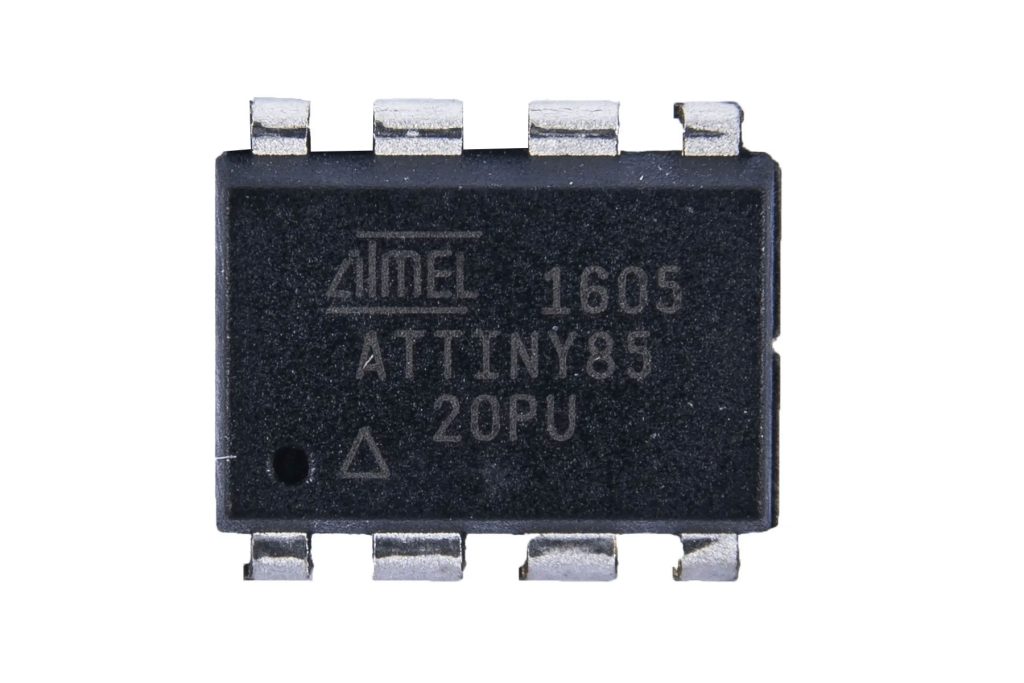
Microcontroller Chip
The ATtiny85 is an 8-bit RISC microcontroller with a clock speed up to 20 MHz (depending on configuration), 8 KB flash memory, 512 bytes SRAM, 512 bytes EEPROM, and a rich set of built-in peripherals.
Form Factor
The ATtiny85 comes in DIP, SOIC, and QFN packages. The DIP-8 version is especially popular with makers due to its breadboard-friendly design.
Built for Simplicity and Efficiency
Despite its small footprint, the ATtiny85 includes:
- 6 configurable GPIO pins
- Up to 3 ADC channels (10-bit resolution)
- 2 timers (1x 8-bit, 1x 16-bit)
- PWM output
- I²C (via USI)
- SPI (via USI)
- Internal temperature sensor
- Sleep modes for ultra-low power
- Internal clock (1 MHz, 8 MHz, and 16 MHz)
ATtiny85 Pinout Overview (DIP-8)

| Pin | Name | Functions |
|---|---|---|
| 1 | PB5 | RESET, ADC0, dW (debugWire), Digital I/O |
| 2 | PB3 | ADC3, CLKI, Digital I/O |
| 3 | PB4 | ADC2, Digital I/O |
| 4 | GND | Ground |
| 5 | PB0 | MOSI, PWM (OC0A), Digital I/O |
| 6 | PB1 | MISO, PWM (OC0B), ADC1, Digital I/O |
| 7 | PB2 | SCK, ADC1, INT0, Digital I/O |
| 8 | Vcc | Power Supply (2.7V – 5.5V) |
ADC – Analog to Digital Converter
The ATtiny85 features three 10-bit ADC channels: PB2 (ADC1), PB3 (ADC3), and PB4 (ADC2). These are ideal for reading analog sensors like light, temperature, or voltage dividers.
Applications:
- Read sensor values
- Measure voltage
- Analog input for user controls (e.g., potentiometers)
PWM – Pulse Width Modulation
PWM outputs are available on PB0 (OC0A) and PB1 (OC0B). Use PWM to control devices like LED’s and motors with variable power levels.
Applications:
- LED dimming
- Servo control
- Soft motor starts
USI – Universal Serial Interface
The ATtiny85 does not have dedicated I2C or SPI hardware. Instead, it uses a flexible USI (Universal Serial Interface) module.
I²C:
- SDA – PB0
- SCL – PB2
SPI:
- MOSI – PB0
- MISO – PB1
- SCK – PB2
Digital I/O
All pins (except GND and Vcc) can function as digital inputs or outputs. Internal pull-up resistors are available and should be enabled as needed for switches or sensors.
Interrupt Support: PB2 supports an external interrupt via INT0 — perfect for responding to button presses or sensor triggers.
RESET & debugWire
Pin 1 (PB5) is the RESET pin by default. It can be repurposed as a digital I/O if reset is disabled via fuse settings — but flashing code afterward will require a high-voltage programmer.
debugWire: debugWire allows single-wire debugging using the RESET pin with compatible tools like Atmel-ICE.
Power and Clock
- Operating Voltage: 2.7V – 5.5V
- Internal Oscillators: 1 MHz, 8 MHz (calibrated), 16 MHz (optional with fuse)
- External Clock: Supported via PB3 (CLKO)
Power Efficiency: The ATtiny85 offers multiple sleep modes, making it perfect for battery-powered applications such as sensors or wearables.
How to Program the ATtiny85
Common Methods:
- USBasp programmer + AVRDude
- Arduino as ISP
- Digispark USB bootloader (6 pins only usable)
Programming Pins (ISP):
| Function | Pin | Description |
|---|---|---|
| MISO | PB1 | Microcontroller to programmer |
| MOSI | PB0 | Programmer to microcontroller |
| SCK | PB2 | Clock signal |
| RESET | PB5 | Controls flash programming mode |
Steps:
- Connect your programmer to the correct pins
- Use Arduino IDE, PlatformIO, or AVRDude
- Set fuses correctly (clock speed, RESET behavior)
- Upload your code

Best Practices and Common Mistakes
✅ Use pull-up resistors on input pins like buttons
✅ Don’t use ADC pins as outputs while reading analog values
✅ Avoid disabling RESET unless absolutely necessary
✅ Be aware of pin sharing (ADC, PWM, SPI overlap)
✅ Set fuses carefully to avoid bricking the chip
✅ Ensure clean, stable power — the ATtiny85 is sensitive to voltage noise
Conclusion: Small but Mighty
The ATtiny85 is the Swiss Army knife of microcontrollers. It fits in your pocket but punches far above its weight. Understanding its pinout unlocks a wide range of powerful applications — from artistic LED installations to energy-efficient smart sensors. Check out my HALLOWEEN – JACK O’ LANTERN project with an ATtiny85!
Happy Building!
Download the ATTINY85 pinout here in high resolution – for free*!
* Free to use under the MIT license — attribution is required.